Dual-Band PCB Antenna Design: Keeping Your EMI In-Line
Table of Contents
If you were born in the 1980’s or earlier, you probably remember those old brick-like cell phones and their giant antennas. Fast forward to the present, and most people don’t even realize that their smartphones have antennas. Proposed antenna designs have come a long way since the 80’s, and new antennas can send and receive in more than one frequency band.
As the mobile and IoT industry continues to advance, electronic devices continue to use wireless communication protocols to send and receive data. These devices will need to communicate in multiple frequency bands to do their job and new antenna designs will continue to make an appearance in PCBs. Dual band antennas pack two antennas into a single module and will help you save valuable space in your PCB layout.
Dual-band Antennas in Your PCB
A dual band antenna is an antenna that can send and receive in two different frequency bands. These antennas can operate on these different frequencies individually or simultaneously, depending on the capabilities of the individual antenna. Standard omnidirectional antenna designs, like a monopole, dipole, or slot antenna, can be modified to show dual-band emission.
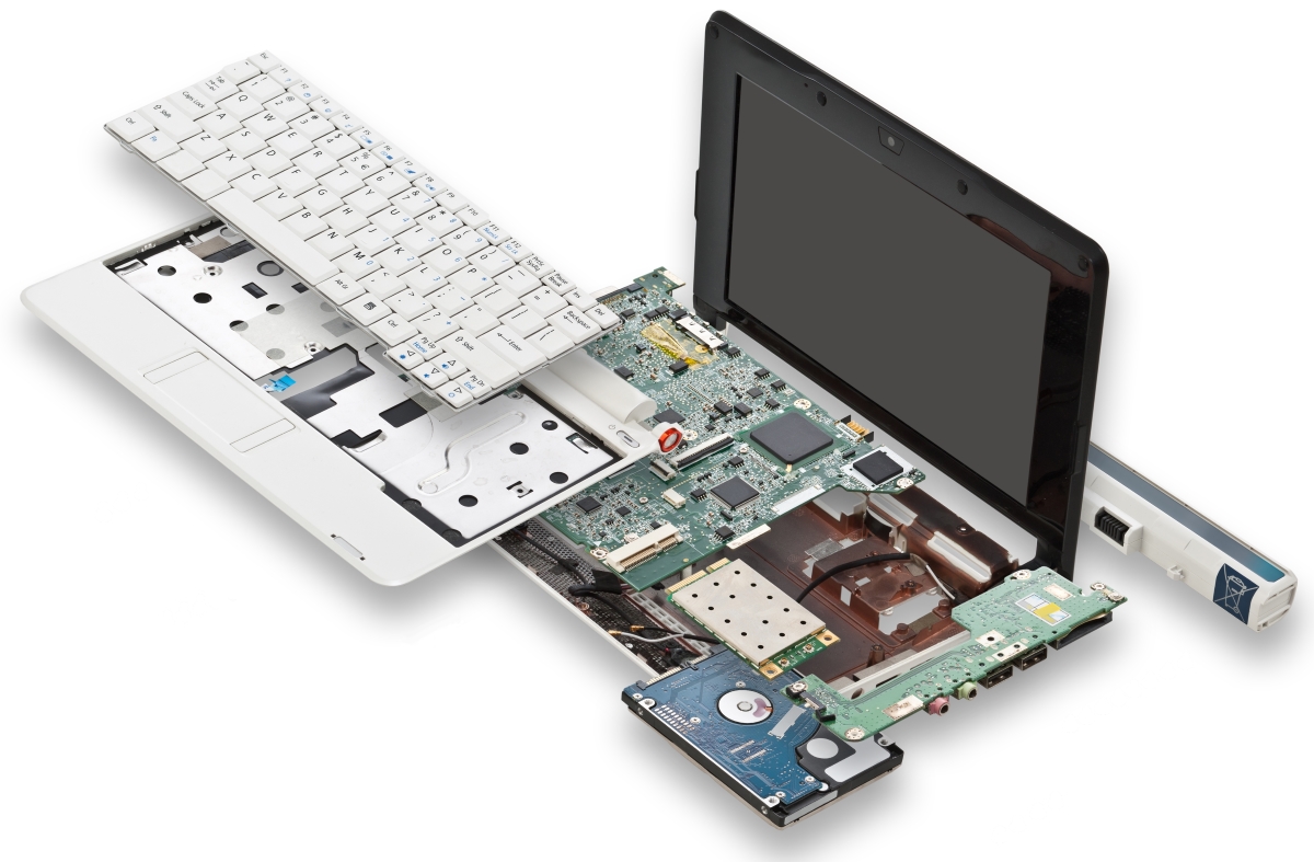
PCB with a dipole antenna module
Dual-band antennas on PCBs are already available that can operate at 2.4 GHz and 5.8 GHz. This type of antenna allows a device to operate according to different IEEE standards and expands its range of communication capabilities beyond WiFi. Some mobile phones use dual-band communication that is separate from WiFi.
Rather than select an off-the-shelf antenna module, a dual-band antenna can be easily integrated into your device. An integrated antenna can be printed directly onto the PCB and has lower manufacturing and assembly costs compared to an external antenna module. As external dual-band antenna modules are printed on their own PCBs, designing and printing your own integrated antenna can help you maintain a smaller form factor.
If designing a printed antenna is not your cup of tea, one other option that maintains small form factor is to use a ceramic chip dual-band antenna in your layout. These chips are low cost and many frequency options are available. They are also impedance matched at 50 Ohms, they meet industry standards, and have high linear gain.
Printed Dual-band Antenna
Printing a dual-band antenna directly on your PCB can be challenging and there are a number of design aspects that should be considered. Any device with high data transfer rate must follow the standard high speed design guidelines.
If your device is going to operate over a wide temperature range, volume expansion/contraction can cause a change in the antenna’s resonant frequency. This changes the power transmitted or received at the intended carrier frequency.
If you use a metal that has a small thermal expansion coefficient, you can minimize volume changes. It is important to match the thermal coefficient of your metal and traces to that of the board material. A large mismatch can lead to delamination or fracture at extreme temperatures.
Once you have decided on a geometry and planned out your design, you will need to match impedance. Most commercially available antennas are already matched to 50 Ohms impedance at 2.4 GHz, and you will need to do the same with your custom antenna. Any impedance mismatch between the antenna and its driver/receiver can be compensated using two inductors and two capacitors.
Basic understanding of a Smith Chart is required for impedance matching antennas. In short, a Smith Chart helps visualize the exact impedance mismatch between an antenna and load. The placement of the inductor and capacitor will depend on the exact mismatch between the antenna and load impedance.
One capacitor/inductor pair will be placed in series with the antenna or load, and the other pair will be placed as shunt elements. Impedance matching of one band affects the matching of the other band, so each band cannot be impedance matched sequentially. Placing your series and shunt elements requires some trial and error and a bit of experience.
When you say you’re a kid at heart, I hope it doesn’t translate to your PCB designs
Self-Jamming EMI
If measures to control EMI are not implemented in your PCB, your antenna may cause self-jamming. Self-jamming occurs when a radiating element (like a radiating oscillator) induces a signal somewhere in the circuit. This degrades the signal-to-noise ratio and can distort the signal sent from a transmitting antenna. This was first termed “self-quieting” in the FM radio community and, more recently, was a serious problem in RFID chips.
Electronic components on your PCB, such as clocks, microcontrollers, and switching power supplies, can cause self-jamming in your PCB and degrade one or both of the signals sent and received by your dual-band antenna. Higher order harmonics in any of these components can produce unwanted emission that interferes with the antenna signal. Likewise, your antenna can cause self-jamming in these components and can degrade signals in the rest of your PCB.
Depending on the arrangement of components on your PCB, shielding may be one option for preventing self-jamming. Be careful not to shield the antenna itself, as transmitted signals will be blocked by shielding and will never reach their destination. If your form factor allows it, critical components like microcontrollers and the electronics supporting your antenna can be shielded, while your antenna is left unshielded on the same board.
Placing shielding may not be appropriate for all designs, especially when the layout is very complicated. When design is constrained by form factor, there are a number of design practices that can help reduce susceptibility to self-jamming and to EMI in general.
Of particular importance is the placement of your clock and its ground plane. It is important to run output traces from your clock over its ground plane in order to minimize loop area, as this reduces any current induces due to stray RF fields. But the ground plane should not be placed directly below the clock itself as this forms a center-fed patch antenna. Eliminating these kinds of net antennas is one of the best ways to prevent self-jamming.
With advanced functionality and an extensive component library that allow you to implement dual-band antennas in your PCB design, Altium Designer can encourage your designing. It also has excellent CAD tools that allow you to design your own dual-band antenna.
If you’re interested in finding out more about how to design with dual-band antennas, talk to an Altium Designer expert today.


