How to Pack More Complexity into a Smaller Footprint Using HDI
Table of Contents

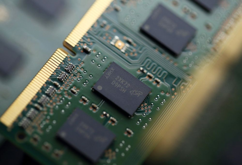
The demand for smaller mechanical housing continues, leading to more complexity in the electrical design process to generate a PCB to keep up with the shrinking form factors. To achieve the size and density necessary, engineers turn to HDI. Using HDI, however, means dealing with different routing workflows, and denser, while using the same area or less. What challenges will you face when using HDI techniques in your own design process?
HDI Design Challenges
Today’s design process often requires engineers to pack as much as they can into as little space possible. Basic design workflows hinder this in a number of ways. Primary among these concerns are the costs of fabrication. Now, it is important to point out, that the fabrication process for HDI designs costs more than a conventional PCB.
Taking processes used for simple through-hole vias simply will not work when creating boards of higher density with higher numbers of connections and components.It seems a bit counterintuitive to expect the design to have more complexity but less workspace to work with.
Here is a basic list of challenges you may run into when designing an HDI board:
-
Limited board workspace area
-
Smaller components and denser spacing
-
Larger number of components on both sides of PCB
-
Longer trace routes creating longer signal flight times
-
More trace routes required to complete the board
HDI Via Styles
At the center of HDI design is the via. Using vias in a different way generates options for routing topology and layout design. Blind, buried, and microvias all have distinct and useful functions in routing an HDI board and Altium Designer® supports all of these. A traditional through-hole via is drilled all the way through the board. The hole is then plated with copper and used for connectivity between layers. These vias then connect to planes, traces, and polygons on the different layers.
Taking this simple concept and now creating vias that start and stop on specific layers, you open up routing options. Another nice option is that if you have ample real estate on the top and bottom layers, but would like to consolidate the board to have fewer layers, it may be possible using different via styles Let’s take a look at some examples of how this would work.
Managing Drill Pairs in the Altium Layer Stack Manager
Altium allows you to manage the drill pairs in the Layer Stack Manager, assigning the start and stop layers for different via types. Starting a via on the top or bottom layer and end the via on an internal plane or signal layer is a blind via. Connecting directly from one internal layer to another internal layer using a via is a buried via. It is also possible to have an isolated layer strictly for routing that is only accessed through buried vias.
Working with Microvias, Pads, and Fabrication
Generating an HDI board can be fairly simple, yet is a powerful method for designing next-generation technology and board design processes. Learn how to incorporate microvias, pads, and fabrication techniques in your next HDI design project by downloading a free whitepaper.
Related Resources


Related Technical Documentation


Take advantage of the world's
most trusted PCB design system.
One interface. One data
model. Endless possibilities.
Effortlessly collaborate with
mechanical designers.
The world's most trusted
PCB design platform
Best in class interactive
routing
View License Options
Thank you, you are now subscribed to updates.