Laser-drilled Via-in-pad Technology in Your PCB
If you’re my age, you probably grew up playing Super Mario Brothers. Whether it’s diving through those green copper pipes, or jumping up through the clouds, moving between worlds in Super Mario is like moving between layers in a multi-layer PCB. Your vias are that critical feature that allows signals to move between different layers. Okay, maybe you there’s less copper and plating involved in Super Mario world, but it’s the same idea.
Via-in-pad design is being more commonly used in PCBs due to the drive towards smaller form factors and HDI design. Placing an annular ring pad around a via reduces the spacing required between components and vias, allowing you to use your PCB real estate more efficiently. Despite the low depth in laser microvias, these structures can be used with via pads, yielding increased component and connection density with better use of valuable PCB real estate.
Laser-drilling for Via-in-pad Design
Since vias are required in multilayer PCBs, designers should decide how vias will be placed in their boards once they move to production. Mechanical drilling provides vias with higher aspect ratio, but the smallest available diameter will be limited in mechanical drilling. Eventually, laser drilling must be used when the via diameter becomes small enough. The same applies to pads used in via-in-pad design.
Working with high pin density components, particularly BGAs or a BGA pad, requires the use of vias as part of the escape strategy. Via-in-pad design becomes required once the BGA pitch becomes very small. BGA pads that are equal to or less than 0.5 mm require laser-drilled microvias as the pad diameter is too small to accommodate mechanical drilling. Laser microvias most commonly span a single layer, resulting in a structure with aspect ratio typically ranging from 1:2 to 1:1.
The low aspect ratios that are easily and accurately accessible with laser drilling makes this process ideal for blind and buried vias. The depth of through-hole vias in multi-layer PCBs results in structures with high aspect ratio, thus through-hole vias are most likely to be mechanically drilled. However, stacking of blind/buried vias allows designers to create a structure that penetrates multiple layers and can still be laser drilled.
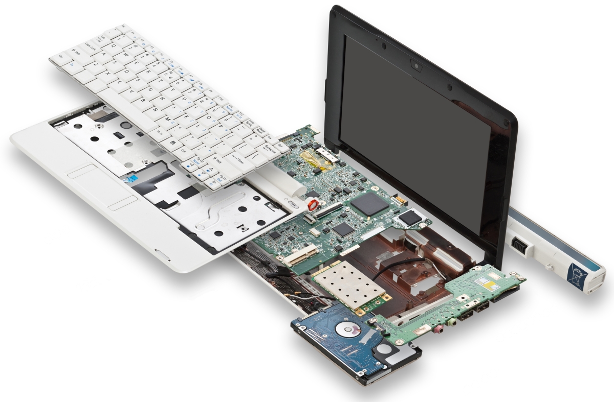
Your PCB might look like a small city when you use laser-drilled microvias
If you elect to use a stack of laser-drilled blind/buried vias to access the inner layers of a PCB instead of a mechanically-drilled through-hole via, it is important to note that each portion of a stacked via structure creates a new inductive discontinuity. This can create a problem with signal reflection and resonance at the interface between each portion of a stacked microvia.
Certain signal frequencies will resonate in stacked vias that are not impedance matched, resulting in significant EMI. Note that this only applies when the total interconnection length (including the stacked microvia) functions as a transmission line. Thus, the use of stacked microvias can be useful when routing signals over shorter distances such that transmission line effects can be avoided.
Cost Tradeoffs in Mechanical Drilling vs. Laser Drilling
Manufacturing costs for PCBs become very important in mid to high volume manufacturing runs. A difference of several pennies per board can add up to a lot of money over time. In deciding to use mechanical or laser drilling, the fixed and variable costs involved need to be thoroughly analyzed.
If you’ve elected to use microvias in your PCB, one aspect to consider is the costs involved in using laser drilling over mechanical drilling. Laser cutters are expensive pieces of equipment, but these systems have a long lifetime. Mechanical drills are cheap, but they wear out quickly and need to be replaced. So when should each of these methods be used?
The right method for placing vias in a PCB mainly depends on size and substrate material, but there is also a cost trade-off that is related to hole density. Standard FR-4 with about 0.1 mm outer diameter via holes can be mechanically drilled with a CNC machine. Laser drilling can still be used for vias with larger diameter. However, there is a cost tradeoff that occurs once the hole density reaches a certain level.
When one examines the production costs associated with mechanical drilling compared to laser drilling, one finds that costs for mechanical drilling tend to outpace laser drilling once the hole density increases past a critical level. Costs increase linearly with the number of vias that need to be placed on a board. Mechanical drilling has lower fixed costs than laser drilling, while laser drilling has lower variable costs.
The primary reason for this cost difference is the tooling costs involved in mechanical drilling. Drill bits wear out and eventually need to be replaced, while laser drilling does not incur these variable costs. At some point, there is a critical hole density where the two drilling methods will have the same total cost. For 0.1 mm microvias, the critical density is about 10 holes per square dm. Laser drilling will have lower total costs at higher via density.
Industrial laser cutter
The above cost tradeoff still applies to via-in-pad design. Once vias are placed in pads on a PCB, they either need to be filled with conductive paste and/or tented with a solid layer of conductor to prevent solder wicking through the via. Via-in-pad plated over (VIPPO) structures can also be used to prevent solder wicking.
Whether you plan to fabricate vias in your PCB mechanically or using laser drilling, you need PCB design software with ultra-accurate CAD tools. CircuitStudio® gives you access to the best layout, simulation, rules checking, and deliverable generation tools. Talk to an Altium expert today if you want to learn more about how can help you reach your design goals.


