Meeting Standards: IPC 6012 Class 3 Via Sizes and Annular Rings

Table of Contents
Take a look at the above image of a PCB layout, specifically the vias and drill holes poking through the silkscreen. It's quite clear that some of these vias are off-center, meaning the drill hit that created these vias was not dead-center in the receiving land. This leaves behind an annular ring, something which might be considered a defect in certain IPC product classes. Under the IPC standards for rigid boards, we have several possible fabrication characteristics that could be considered defects in different types of boards (HDI, flex, etc.); annular rings are just one of many possible structural characteristics that could be considered defects.
Designers often conflate leftover annular ring and pad sizes, something for which I am guilty of. However, the two are related; designers need to place a sufficiently large pad size on the surface layer to ensure that the annular ring that is leftover during fabrication will be large enough. As long as the annular ring is sufficiently large, the drill hit will not be considered defective and the board will have passed inspection.
In the IPC-2221 standards, annular rings are applied universally for Class 1-3 products. In the newer IPC-6012 standards, breakout is allowed for all but class 3 products. In this article, I'll discuss the limits on IPC-6012 Class 3 annular rings as these are a standard fabrication requirement for high-reliability rigid PCBs.
IPC-6012 Class 3 Annular Ring Size
The IPC standards define three product classifications (Class 1, Class 2 and Class 3) based on the required level of device reliability. Each of these classes carries its own guidelines performance and qualification requirements for fabrication, cleaning, and inspection of PCBs. Issues such as component placement, via hole plating, residual contaminants, trace sizes, and other considerations in the PCBA are all addressed in the standards for each of these classes.
In order for a fabricated plated through-hole via to be accepted after fabrication, we have to ensure that the leftover annular ring in each IP Class will be sufficiently large. Therefore, the exercise of "sizing" an annular ring is really one of picking the right land size for your via. As long as your lands on your vias are large enough, then you have successfully accommodated fabrication tolerances in your PCB.
Annular Rings Visualized
The diagram below shows how a leftover annular ring arises during drilling in the PCB fabrication process. The image on the left shows breakout, which is allowed under the IPC-6012 standards but not under the IPC-2221A standard. IPC-6012 is the primary qualification standard in use for rigid PCBs, so it should be considered when sizing pads and vias, and the Class 3 annular ring limits are consistent across the two standards.
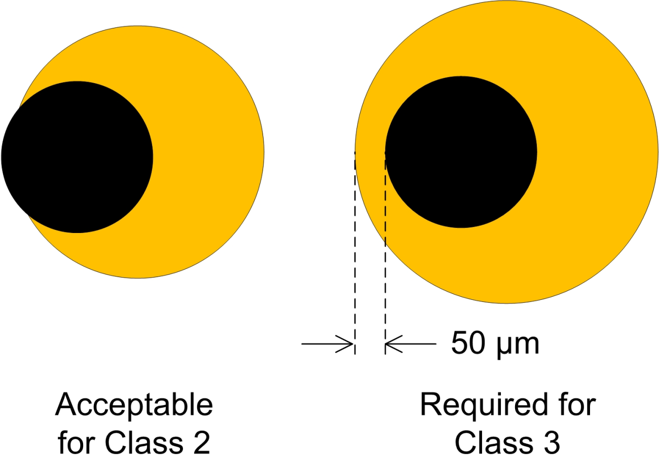
The annular ring is measured in two ways for external and internal layers:
- For external layers, the annular ring is measured from the edge of the via wall plating to the edge of the pad.
- For internal layers, the annular ring is measured from the edge of the drilled hole to the edge of the pad.
This means the two values will be different by the plating thickness, which is a minimum of 0.8 mil for Class 1 and 2, or 1 mil for Class 3. Most fabricators will plate unfilled plated through-hole vias slightly thicker than the minimum Class 3 plating thickness of 1 mil in their products (see Table 3-2 in the IPC-6012 standard for minimum hole wall plating requirements in mechanically drilled holes).
Minimum Annular Ring Size Requirements
Under IPC-6012, Class 3 products require some leftover annular ring, while Class 1 and Class 2 products allow some breakout.
|
|
|
|
|
|
|
|
|
|
|
|
|
|
|
|
As we can see, according to IPC 6012 standards, only Class 3 carries an appreciable annular ring requirement. To ensure some level of reliability on Class 2 and Class 1 products, I like to state that the leftover annular ring should be 0 mil (internal layers) or equal to the plating thickness (external layers). This will cause you to meet a tangency condition where the annular ring just touches the edge of the pad, so there will be no breakout and the design will be considered fabricated successfully.
Calculating Pad Size From Annular Ring Size
The pad or land size can be calculated with the simple equation L = a + 2b + c, where a = drill hole (internal) or finished hole (external) diameter, b = minimum annular ring size, and c = fabrication allowance. Think of c as the allowed wander in the CNC drill. Most fabricators will (or should) aim for Class C fabrication allowances, which is the highest classification and carries a limit of c = 8 mil (see Table 1.6.3 in the IPC-2221 standard for fabrication allowance classifications). From the above table and formula, we can now calculate the annular ring requirement for an example 12 mil via.
Suppose you want to place a 12 mil diameter via in a Class 3 product. According to the above plating requirements I mentioned, the finished hole will only be 10 mil diameter. With these values, we can now calculate the minimum annular ring size for a Class 3 product, assuming a Class C fabrication allowance. We would have:
- Internal layer minimum pad size: L = 12 mil + (2 x 1 mil) + 8 mil = 22 mil
- External layer minimum pad size: L = 10 mil + (2 x 2 mil) + 8 mil = 22 mil
So we can see that, because the plating is set to a minimum of 1 mil, we can set the minimum via land size to (via diameter) + 10 mil for all layers. This is regarded as the "safest" approach to sizing vias and pads so that you comply with IPC-6012 Class 3 annular ring requirements.
What about Class 1 and 2 pad sizes? Take a look at these guidelines:
- For Class 3 products, we take b = 2 mil for external annular rings and b = 1 mil for internal annular rings
- For Class 1 and 2 products, we would technically have b < 0, so to be safe you should size the pad using b = 0 internally and b = via wall thickness (1 mil) in the above formula
Therefore, if we just require 1 mil hole wall plating thickness in all classes, we could comfortably say that the via land size is (via diameter) + 8 mil.
Summary and Teardrops
Hopefully, this illustrates a basic safest-possible guideline a designer can follow when placing vias and selecting pad sizes. The (via diameter) + 10 mil for Class 3 and (via diameter) + 8 mil for Class 1/2 guidelines will be fabricable by probably every manufacturer on the planet, and this is the approach I take when sizing vias and pads.
Just for added reliability in Class 3 products, I always add teardrops to via pads, especially when the trace is thin and there is a risk that the drill hole will sever the trace from the pad. This provides an extra measure of reliability that you might need when routing on an internal layer with controlled impedance traces. Such an example situation might require thinner traces to hit your impedance target, and adding the teardrop to the via pad is an easy way to ensure reliability rather than decreasing the hole size. At some point, with thin dielectrics and thin traces, you can't decrease the mechanical drill size anymore and you will have to use teardrops to ensure reliability.

Via-in-Pad and IPC-6012 Class 3 Requirements
At even higher density, you may need to use via-in-pad in order to route into components. Via-in-pad can technically be used in general without plugging and capping, but the best practice from an assembly and reliability standpoint is to plug and cap. The main standardized via types that could be plugged and capped are specified in IPC-4761, as outlined in this article. The list of via types in the linked article are just standardized definitions for vias, but not all of these are considered acceptable per Class 3 requirements.
The Class 3 requirements for via-in-pad are listed below. The values used here are adapted from the Class 3 requirements listed above with minor variations.
- Filling material: Vias should be filled with a non-conductive epoxy.
- Capping and plating: Vias should be capped and plated over.
- Cap thickness: Cap plating should be a minimum of 12 microns (0.472 mils).
- Protrusion/planarity: The in-via protrusion cannot be more than 50 microns (1.96 mils). This may require a planarization step.
- Minimum drill size: Drilled holes in pads must be at least 150 microns (6 mils).
- Minimum pad size: The minimum pad size is the drill diameter + 0.010").
- Pad clearance: Via-in-pads should be at least 6 mils away from adjacent copper features, including other via-in-pads.
- Minimum annular ring: The minimum copper surrounding the via hole is 2 mils.
When via-in-pad is used in a PCB layout, the plug and cap definitions also need to be delivered to your fabrication house. Plug and cap processing can be used in the entire PCB if desired, or it can be confined to specific locations where via-in-pad is being used. In either case, those location requirements need to be communicated to the fabrication house.
This can be done easily by including the fill and cap information as Gerber exports. This is normally done by creating a Gerber layer with the fill data, and another layer with the cap data. These options can be added to your Gerber exports, ODB++ exports, or IPC-2581 exports when configuring your output files. An example with Gerber exports is shown below.

Once the Gerbers/ODB++/IPC-2581 data is exported, the plug/fill/cap data can be viewed in a CAM application. This data will show up in its own layers, and the process engineering team at your fabricator will be able to see which specific vias require filling and plating. The data will look similar to mask opening but will match the hole size being placed during drilling, so don't confuse this data for a mask opening when reviewing the Gerber files.
Finally, make sure to include a fabrication note stating the following if you are going to use via-in-pad with any of the standard IPC-4761 via types:
- Vias in Gerber layer (LAYER EXTENSION) shall be fabricated according to IPC-4761 Type XXXX standards.
- Vias shall be filled with non-conductive epoxy.
- Vias shall be plated over. Resulting protrusion not to exceed XXXX mils per IPC-6012 Class 3 requirements.
When you need to design your PCB vias and routing to ensure you comply with IPC-6012 Class 3 annular ring standards, use the padstack design and routing features in Altium Designer®. Once your design is ready for a thorough design review and manufacturing, your team can share and collaborate in real time through the Altium 365™ platform. Design teams can use Altium 365 to share manufacturing data, project files, and design reviews through a secure cloud platform and in Altium Designer.
We have only scratched the surface of what’s possible with Altium Designer on Altium 365. Start your free trial of Altium Designer + Altium 365 today.

About Author
Related Resources


Related Technical Documentation


Take advantage of the world's
most trusted PCB design system.
One interface. One data
model. Endless possibilities.
Effortlessly collaborate with
mechanical designers.
The world's most trusted
PCB design platform
Best in class interactive
routing
View License Options
Thank you, you are now subscribed to updates.