What is PCB Star Grounding and Why Would Anyone Use It?

Table of Contents
If you look on the internet, you'll find some interesting grounding recommendations, and sometimes terminology gets thrown around and applied to a PCB without the proper context or understanding of real electrical behavior. DC recommendations get applied to AC, low current gets applied to high current, and vice versa... the list goes on. One of the more interesting grounding techniques you'll see as a recommendation, including on some popular engineering blogs within the industry, is the use of PCB star grounding.
The term is not exclusive to PCB design, and it gets used in a variety of contexts that do not deal directly with defining ground on the PCB. It is a systems analysis term, and it seems that the term has been applied to PCBs without much attention to the practical aspects of making ground connections in a real circuit board. There are some layouts where you can mimic a star ground, but this ends up being an impractical exercise when you start thinking about it. The proper way to design on the board is to use ground planes, except in some cases where you have little or no control over return paths, or where you need isolation.
Although implementation of star grounding in a PCB is difficult and not always necessary, it is something that is done, in a way, in home, commercial, or industrial wiring. In a multi-board system, possibly one that requires isolation or long links over cables, you can also implement some interesting designs that follow the PCB star grounding philosophy, just on a somewhat larger scale. Let's look deeper at this idea of star grounding; we'll see an instance where this method of grounding can be applied in a PCB under certain conditions.
What is Star Grounding?
Star grounding is normally used to connect multiple modules, instruments, or some other equipment to a single grounding point such that they all have the same potential. The groups daisy chained plugs used in residential wiring are basically arranged in a star configuration with earth as a safety and ultimate reference point. The same idea is often applied to multiple modules or instruments that are connected to the same power circuit, similar to residential wiring (without daisy chaining).
When this term gets applied to a PCB, it encourages the use of a grounding strategy that is bad for routing (especially impedance controlled routing), bad for EMI, and is often bad for power distribution. There is one case where you can create an EMI-free mixed-signal system by implementing a star ground in a PCB, but this ends up being a trivial case that provides no benefit to the designer. There is also an analogous multi-board design case involving star grounding, but this has the same topology in the above arrangement. Other cases like DC or low-current, low-frequency analog/audio might be appropriate for star grounding on a PCB, but it depends on what other functions might be included in the system.
Clearly, star grounding is not for everyone or for every design, yet I continue to see it recommended as a cure-all for EMI problems, including in mixed-signal systems. So why is this still recommended in a PCB, even though it was not really intended for use in a PCB?
Why Would Anyone Recommend Star Grounding in a PCB?
There are two reasons people continue to recommend star grounding in a PCB. These are: providing isolation between digital and high frequency analog, and preventing ground loops. Let's examine both of these points.
You Don't Need a Star Ground for Isolation
This recommendation dates back to a longstanding bad design guideline: you should place splits or cutouts in planes to prevent high frequency and digital interference. This guideline is bad for routing and bad for EMI, and in particular it leads to awkward layout choices that don't always make sense.
The idea in star grounding is to put a high impedance obstacle between the return path from one type of signal (DC, low-frequency AC) and another type signal (high speed, high frequency, etc.), or between two different circuit groups that you want isolated over their own ground polygons. I can see three cases where this might make sense:
- Circuit blocks are totally isolated and only share a single ground connection at the supply; there is no routing between each section or interfaces bridging each section (no A/D or D/A converters, etc.)
- You're using DC or very low speed signals (slowly charging/discharging RC circuits), particularly when ensuring high SNR values is critical (precision measurement is one example)
- You need to separate low-level, low frequency analog signals (meaning kHz or lower frequencies) from a low-speed or high-speed digital section
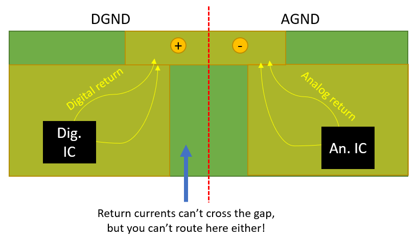
Aside from these specialty cases, you generally can't justify the use of star grounding in a PCB due to EMI and crosstalk concerns. With a star ground involving any digital signals, you can't route between board sections as you will create significant radiated EMI. Essentially, any signal that you route across the gap between the two sections will encounter a very high inductance loop that defines its return path.
If you're dealing with MHz or higher frequencies, and you're using digital signals that need to be routed into some interface near the analog section, you won't need a star ground if you're smart about the way you layout the board. Return path isolation will be a non-issue; return paths will naturally couple capacitively near traces, rather than spreading out in the ground plane. Properly sectioning analog and digital circuitry and components into different regions above a continuous ground plane is the best choice here.
Regarding case #2 above, this is fine as long as the interconnect and board are totally shielded, but it's the wrong move if sensitive measurements that have high noise immunity are required. In this case, board-level and enclosure-level shielding might be the answer as you can get to high shielding effectiveness.
Star Grounding in a PCB is Meaningless for Ground Loops
The other reason that star grounding is recommended in a PCB is to eliminate ground loops, or rather to prevent them from existing in the first place. If your design has a problem with ground loops, there is some other problem in the design that can't be solved by star grounding. This is another area where PCB design has adopted terminology from other areas of electronics and used it in ways it was never intended:
- PCB designers sometimes refer to a ground loop as a literal loop that carries a return current. This can arise via (a) GND net traces being routed in a big circle, or (b) in multipoint grounding through plated PCB mounting holes to an enclosure. 99% of the time, you won't notice a ground loop because a potential difference between a single GND section is so small. It becomes very important when dealing with very low level signals, such as high impedance sensors operating at less than 1 uA of current.
- Power systems engineers use this to describe unintended current flow in grounded/earthed systems, which might be separated by long distances (not on the same PCB). You'll often see this mentioned regarding utility grounds poles that are literally connected to the earth. Due to the non-zero resistance of these earth connections, it should be no surprise that ground potential offsets can arise between equipment connected to different grounding points.
Ground loops as described in #2 can occur in a PCB as described in #1 (b), where there are two connections between a given ground net and the enclosure, or when GND on two different layers are connected with high impedance connections, and there is a non-zero potential between them
On the PCB, you have an analogous situation, just at smaller scale, which can occur in only the digital section, only the analog section, in both sections, or between both sections (when the enclosure is involved). An example occurring only in the digital section of our hypothetical star ground PCB is shown below.

This problem in separated equipment is one of the primary motivations for using differential signaling over long cables rather than using groups of single-ended signals in long shielded cables. Shielded cables are fine over short runs that don't experience high ground offset. However, when the shields are connected to grounds at both ends, and there is a ground offset, your shielded cable is now carrying a current in a ground loop! This is a safety concern as someone who grabs the shielding or chassis connection on either side could create a path to ground and get a shock, or the cable could burn up.
On the PCB, we practically don't have this problem unless you have high impedance in your ground connections that create some ground offset potential in the ground plane. One place where this might happen is in the enclosure, where you're using multipoint grounding in the wrong situation (e.g., in high current DC rather than for RF). It only becomes a safety problem when:
- All multipoint ground connections in a single ground region have high impedance to whatever ground return is in the system
- The system is operating at high current
- The user interacts and can touch the conductor carrying the ground loop
Note that I haven't even brought up the possibility of different ground regions: it's all within the same ground region (single plane). The point is; you can have star grounding and ground loops, but if you have ground loops that are causing signal integrity problems, then there is probably a different set of problems that can't be solved with a star ground. For most PCBs, your main problem with ground loops will be some broadband noise that could interfere with low-level analog signals (usually from some sensor), leading to high SNR in any sampled signal and inaccurate data.
Take a Grounded Approach
Well-designed PCBs have ground circuits that rely on a precise approach for providing a low-impedance return path for current. To counter noise, a design could rely on a ground plane as a return current path. Do not place any break between the analog ground region and the digital region to achieve isolation. The one exception is at audio frequencies, when you need to separate DC power from everything else, and if you happen to only be working at DC everywhere in the board. I'm sure there are some other low-frequency exceptions that exist.
For the majority of designs with a digital section, you should focus on laying out the board properly over a ground plane, rather than split up ground regions and create a star ground arrangement with bad routing. You can read more about the various cases involved in grounding and problems with star grounding in this article. As you'll see, the main case in PCB design where star grounding is acceptable is completely trivial; you gain no benefit by implementing it and you might as well put each section of the design into its own board. If you layout the board properly, you'll be able to reduce radiated EMI through proper routing.
You don't need to resort to outdated tactics like star grounding when you use the best PCB design software. Use the complete set of design, layout, and stackup creation features in Altium Designer® to create and route your physical layout. When you’ve finished your design, and you want to release files to your manufacturer, the Altium 365™ platform makes it easy to collaborate and share your projects.
We have only scratched the surface of what’s possible with Altium Designer on Altium 365. Start your free trial of Altium Designer + Altium 365 today.

About Author
Related Resources


Related Technical Documentation


Take advantage of the world's
most trusted PCB design system.
One interface. One data
model. Endless possibilities.
Effortlessly collaborate with
mechanical designers.
The world's most trusted
PCB design platform
Best in class interactive
routing
View License Options
Thank you, you are now subscribed to updates.