Utilizing Layout Options for Rigid-Flex Design
Table of Contents
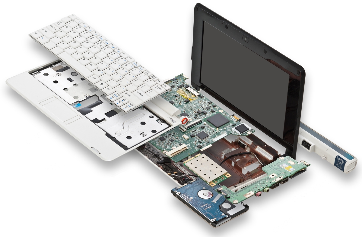
If you own an electronic device that folds, bends, twists, or deforms in some way, it most likely contains a rigid-flex PCB. These circuits contain many of the elements in any PCB, like traces, vias, and even components mounted on a flexible ribbon. However, getting started with a comprehensive design for these circuits requires the right software specifically built for rigid-flex boards.
Form factors are becoming more specialized and demanding. Industrial systems, complex instruments, and plenty of other systems require multiple boards with odd form factors. Building PCBs for these systems requires software that seamlessly integrates multiple design modalities into a single, intuitive interface. Only design software with an integrated design environment weaves these design tools into a single process and gives you the flexibility you need.
Layout for Rigid-flex Design
Rigid-flex design and multi-board design are joined at the hip by a flex ribbon. The only difference between the two types of designs is the presence or absence of flex ribbons. Rigid-flex boards use a ribbon, while boards in a multi-board connect using a connector and a cable.
One great way to design both types of systems is to use a hierarchical schematic design. You can separate different functional blocks in your system into separate schematics, and then link these schematics together using hierarchical schematics. Schematics will be organized into “levels”, where each lower level is a schematic for a different function in the system. Think of it as linking multiple schematics together like puzzle pieces inside of a larger schematic.
Once you’re ready to layout your board, you need to define which boards contain different functional blocks in your system. Doing this the right way requires design software with a straightforward layer stack manager. Your stack manager defines the material arrangement in each rigid and flexible portion of your PCB.
Separating functionality onto different boards based on functional blocks has another advantage in terms of designing your layer stack. You can use this to determine the number of layers you need in each rigid and flex section of the board. This is important as it gives you an opportunity to save on production costs by using a smaller number of layers in certain rigid areas of the board. Some boards in the system may have dense layout and routing requirements, while portions of the system will operate just fine with fewer layers.
Once you have your layers defined and the flex PCB is arranged, you can capture different schematics into different rigid and flexible portions of the board. Your routing tools should allow easy routing across the flex ribbon just as you would on a rigid board. This should include allowing you to place components in the flex zone and route between signal, power, and ground layers in your flex ribbon.
A rigid-flex board as a multi-board system
Realizing Where the Pain Comes From
The most important part of the rigid-flex design is the definition of your layer stack in each portion of your system. This requires an intuitive layer stackup manager that makes it easy to define rigid boards and flex ribbons. Your stackup manager needs to be part of the electrical design workflow by allowing you to differentiate between power, ground, and signal layers. This makes your interactive routing tools much easier to use as they can automatically reference to the appropriate ground plane.
Once you define the various rigid and flex zones in your board, you’ll need schematic capture tools that create an initial layout in each portion of the board. Working with hierarchical schematics shouldn’t require a convoluted folder structure to order your schematics. Each schematic should be referenced within its higher level schematics, making it easy to locate and reuse your existing schematics in new projects.
When a flex zone connects directly to a rigid rigid zone in the interior of the rigid board, you’ll need to define a transition zone between the flex ribbon and the board. Some software programs create a special process for defining this important zone. There is no reason for this because the transition zone has a slightly different stackup than your flex region. You should be able to do this within the all-important stackup manager.
Verifying your board flex and overall form factor takes 3D visualization tools that are built into your PCB design software. You shouldn’t have to export your design to another program or replicate it in an MCAD module. Your electrical and mechanical design teams should be able to collaborate on your design within a single program. Other PCB design platforms don’t have these tools, or they place them in an external module. These other platforms force you to use another program like SolidWorks or AutoCAD to get a 3D view of your design.
Designing Rigid-flex Boards the Right Way
Rigid-flex design starts with designing the layer stack for your rigid board, your overlays and polyimide layers, and your flex ribbon, as well as the link between the different types of layers. These tools should be adaptable to any multi-board system. Drawing your board outline should be as intuitive as the tools used in any CAD program, and you should be able to capture different schematics into different sections of your system.
When you’ve finished your design and you are ready to work with your mechanical team on packaging, you shouldn’t have to move between two or three programs to start designing packaging for your board. If your PCB design software integrates your rigid-flex PCB design tools with MCAD features, you can collaborate directly with your mechanical design team in a single program.
When designing multi-board systems with rigid-flex portions or an entire rigid flex system, make sure to check with your manufacturer before defining your stackup and before placing components directly on a flex ribbon. You’ll need to decide whether your flex ribbon will be dynamic or whether it will remain static. You’ll also need to check on the allowed layer count and thickness that can be used in your ribbon. Your manufacturer might send you a pre-built stackup file that matches their capabilities.
If your manufacturer does send stackup files defining their stackup requirements, your design software should be able to import and reuse these stackup files. This saves you time as you won’t have to define your stackup manually, and you can rest assured that your board will meet your fabricator’s capabilities.
Rigid-flex design tools in Altium Designer
Rigid Flex Design in Altium’s Unified Design Environment
Altium design model integrates layer stackup management, layout, advanced routing, and design rule checking features in a single, unified design environment. The powerful CAD tools, layout options, and customizable routing and via tools make it easy to build any rigid-flex PCB. The ultra-accurate 3D viewer integrates ECAD and MCAD design, helping facilitate collaboration among multiple team members and enhancing your overall design process. All these design features are easy to locate within the program.
The great thing about working with an integrated design platform like Altium is that rigid-flex, multi-board, and multilayer design all use the same tool. Working with the layer stackup manager allows you to define various board regions, and the hierarchical schematic features make it easy to link various functional blocks in your device to different board regions. You can quickly import your schematics as initial layouts in any section of your system.
Without question, the best PCB designs software package for rigid-flex, multi-board, multilayer, and HDI design is Altium. The rigid flex design features are inherently integrated with the multilayer and multi-board capabilities, and the beautiful design interface makes visualizing your layer stack easy. The MCAD/ECAD collaboration features allow you to view the mechanical folding performance of your rigid-flex board and aids packaging design.
Altium never wants to see their customers fail, and they back it up by providing you with the resources you need to succeed. Altium gives you access to useful design examples, thorough documentation, and product extensions to expand your range of capabilities. You’ll have access to the AltiumLive forum, video, user groups, podcasts, and webinars provided by industry experts. This dedication to customer success set Altium apart from other PCB design software companies.
If you’re interested in playing with Altium, you can download a free trial of the PCB layout software and see if it’s right for you. Talk to an expert at Altium today if you want to learn more about Altium and its rigid-flex design capabilities.


