PCB Ringing: What Causes and How to Reduce Ringing In Circuit Boards
Table of Contents
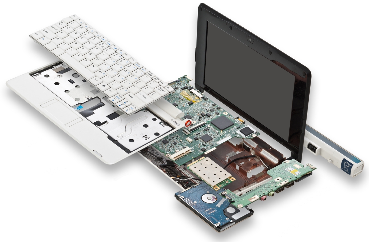
Digital circuits are particularly sensitive to ringing effects. Editorial credit: Dikiiy / Shutterstock.com
In my very first electrical engineering lab, we built a printed circuit to debounce the output of a switch. I remember seeing the original jumpy signal and then the debounced output on the screen of an oscilloscope. I felt a profound sense of unease that something so innocuous in our lives could be so...messy. It’s a good thing that my freshman self didn’t know that was just the beginning of my distress over signal frequency noise and artifacts. Signal ringing is one of those effects that can be particularly frustrating for product performance.
What Causes Signal Ringing on a PCB?
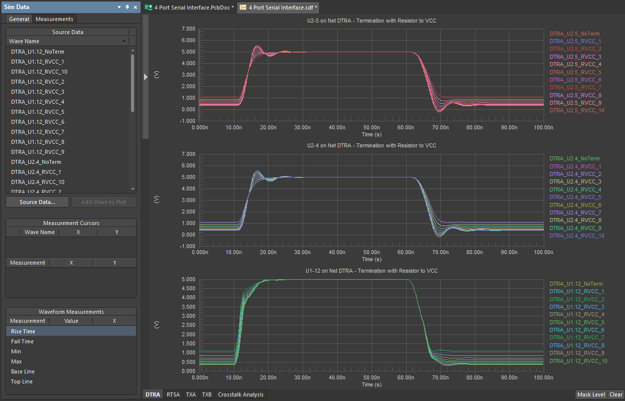
When we’re talking about a Printed Circuit Board or other electronic systems, ringing is a voltage or current output that oscillates like a ripple on a pond when it’s seen on an oscilloscope. The oscillation is a response to a sudden change in the input signal, like turning it on or switching.
The oscillation often takes the output signal frequency out of tolerance on both the high and low ends and gradually smooths out. The time it takes for the oscillations to fall within a tolerable error range is called the settling time.
Because of the characteristic shape of the output signal, ringing is sometimes called “ripple.” However, ripple usually refers more specifically to output when using AC switched power supplies, if the supply doesn’t properly or adequately suppress the AC waveform.
What causes ringing in cross-linking agents?
The source of ringing, besides power supplies, depends on whether your traces are “long” or short. A rule of thumb is that traces are considered “long” if the round trip propagation time (to the load and back) is comparable to the signal rise time in printed circuits. If you happen to be working with striplines or microstrips, it’s a little more complicated and I recommend Glen Dash’s page as a starting point for line length and minimizing transmission line effects like ringing.
Back to long and short traces… If you have a short trace, ringing is caused by parasitic inductance and capacitance. A pulse or sudden change in the input causes the parasitic components to resonate at their characteristic frequency domain, creating the ringing effect in your output. On long traces, the cause of ringing is more likely to be signal frequency reflection from an impedance mismatch.
Signal noise caused me a disproportionate amount of angst as an undergraduate, but it can have catastrophic consequences once you’re in the industry.
How does signal ringing affect my multilayer circuit board?
If you don’t suffer an existential crisis because of a noisy oscilloscope, that’s great. You’ll have much lower therapy bills. Even so, ringing can have negative impacts on your life and product design.
Increased EMI: Ringing can, and often does, produce noise and interference. This can radiate or conduct across your ground plane, with all the associated performance problems.
Increased current flow: Ringing causes increased current to flow through your circuit. Not only does that cause a corresponding increase in power consumed by your product (and shorter battery life), but the components on your ground plane will experience additional, unexpected heating. That can decrease their functionality and lifetime.
Decreased performance: Along with the accumulated performance drops from the increased current and heating, ringing decreases performance across a range of metrics. Because you have a lag in output due to the settling time, the vias and responsivity of your circuit board will drop. The resolution of your outputs will also be much poorer.
If you have digital circuits, ringing is especially damaging. You still have all the problems we’ve covered, and the threshold is much lower. Combine this with any supply rail noise, and you’re likely to have errors and corrupted data.
Audible feedback: A special case of ringing occurs in audio and video applications. Ripple occurs in the audible range and will be heard in your output. It also creates visible artifacts in video displays.
In audio and video applications, ringing can audibly affect your outputs.
How do I prevent signal ringing in a PCB?
Signal ringing can vary from annoying to catastrophic in your system performance. Optimizing your design makes a huge difference in the performance and output. First, you want to reduce parasitic inductance and capacitance. You should minimize node lengths, especially around power stage components on your ground plane. You also want to use impedance matching to minimize any signal reflection. Impedance matching varies with your application and I recommend starting with the Texas Instruments technical articles for very specific advice on a range of applications.
While it’s impossible for any existing program to check for every source of possible interference, having a good one can offload a lot of the work. That leaves you free to deal with the most important challenges, instead of playing design whack-a-mole as you optimize all the parameters of your circuit board. Altium Designer makes some of the best PCB software, like Altium Designer®, and has tools for taking a lot of that error-checking load off your shoulders. This gives you time to contemplate the philosophical implications of noisy circuits. Or you can just get on with your life.
Have a question about ringing? Contact an expert at Altium Designer.


