Step Up Your Game: Multi-Board Versus Multilayer Designs

Table of Contents
Sometimes, a circuit board gets too cramped and has too many layers for its good. Highly cramped assemblies and higher layer counts generally increase costs, and you can't always enlarge a board just to fit everything into your mechanical constraints. Things like enclosures, connector placements, attached mechanical or electrical components, and the like all limit what you can do inside the space you are given. What's the difference between a multi-board vs multilayer design?
If the component and function counts in your system start to increase, what are some ways you can add this to your design without cranking up the density and layer count? One option is to use a multi-board assembly, where the additional functionality is placed on a second or third board. Getting it right involves selecting the right connectors, cables, and stack up for each board, but this can help you ensure you get all your required functionality into one system without significantly higher density and layer count on a single board.
What Can Drive Higher Density and Layer Count?
Many factors can force you to use more layers in your PCB or to place parts on a separate board and link your PCBs together. An additional board cannot always solve extra layer count problems, and adding extra layers cannot always solve an additional board problem. However, there are some instances where each approach is entirely necessary. Some of the biggest drivers of higher layer count are the requirement for additional ground, power, or signal routing, and this is usually to accommodate more advanced components. The other extreme is a change in the design that requires many more components; unless you're putting cavities into the PCB, you won't solve higher component count problems with higher layer count.
On the other extreme, an additional board can be just what the doctor ordered if the component count increases in your design. This is especially true if your board size has a hard mechanical constraint that prevents a board size. In this case, where you have to increase component count with new circuitry or design modifications, you're only option is to go with an additional PCB.
Let's look at some of my favorite examples where we have to add a board or layer.
Going Multi-Board
If your board is getting more diverse in its functionality, or you need to integrate different types of subsystems into your product, then a multi-board approach will probably be best. This can also be driven by mechanical requirements in your enclosure. Here are some instances where you will find multi-board preferred over high-layer count boards:
Prefer to avoid a hybrid stack-up. Hybrid stackups can be unreliable if your fabricator does not know how to build and qualify these. Hybrid stack-ups could also be more expensive than just adding a board, depending on the materials being used. If you want to avoid a hybrid stackup approach, you could always just use the hybrid layer as its own board. This is an approach I have taken in RF systems in the past, where the more advanced RF section lives on its own PTFE PCB.

RF power amplifier module created in Altium Designer. Read more about this project.
Different power requirements. Power is one particular area where it is extremely common to see a supply dedicated to its board or module. Power supply modules are available from many vendors and they are typically built to output standard voltages. If you have a custom power supply, you can take the same approach and place it on a separate board that attaches to your host PCB with a mezzanine power connector or pogo pins. This gives you a convenient module form factor and the customization you might need for your particular power supply.

Non-isolated power supply module from Texas Instruments.
Replaceable or hot-swappable boards. Sometimes, you may have a requirement for hot swapping of add-in PCBs or making a board replaceable. Dedicating this circuitry to a second board gives you much more freedom in terms of how you design the rest of your system. That second board can be connected to the host board with mezzanine connectors or headers. Another option for connecting two boards with data and power is a flex printed circuit (FPC) cable. Some examples where you will find this approach include expansion cards, accelerator modules, and many applications in mobile, and embedded systems.

Camera modules are a great example of an external FPC-connected subsystem.
Adding More Layers
There is another route to go when your board gets too cramped, and that is to add more layers to the PCB stackup. As we saw above, adding another board solves a specific set of problems, and adding more layers solves a totally different set of issues which are typically related to component density.
Higher pin density components. Switching to a finer pitch BGA is a common instance where additional layers will be required. These layers may also need to be thinner because microvias might be needed to support very fine pitch connectivity. Some processors in the same part number grouping can come in different packages, and those different packages might require different stack-ups to accommodate all the pins and fanout routing. A well-known example I addressed in a video is the STM32 in a BGA package:
Dedicated power layer. If the issue to be solved is more copper being allocated for power, then one solution is to place all rails on a new layer. This is an alternative to using an external power module and it works best in the following situations:
- There are multiple rails present at different voltages
- Each rail must provide significant current
- Each rail needs to provide fast current pulses
This is another approach typically seen when a design has a large processor in a BGA package. These components can very commonly require supplying fast pulses and large total currents. For an example of a system that requires this kind of architecture, see the BGA package below.
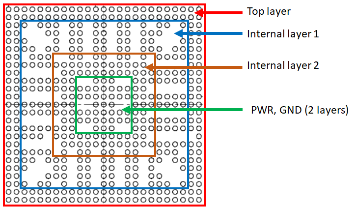
The power region in the inner portion of the BGA can be dedicated to multiple power rails. Read more in this article.
Separating signals. The best way to prevent crosstalk between large groups of signals is to de-densify them. If you've built a board with high densities of signals, and you need to reduce density, then another layer is exactly what you need. This is usually a less costly approach than making the signal layer dielectrics thinner. In addition, we normally wouldn't use an additional board for this approach because we aren't adding more components.
The multi-board PCB design features in Altium Designer® can help you build advanced assemblies and design interconnects between them. If you decide a multilayer PCB is the best path forward, Altium Designer's best-in-class PCB design features have set the standard for usability and excellence. When you’ve finished your design, and you want to release files to your manufacturer, the Altium 365™ platform makes it easy to collaborate and share your projects.
We have only scratched the surface of what’s possible with Altium Designer on Altium 365. Start your free trial of Altium Designer + Altium 365 today.

About Author
Related Resources


Related Technical Documentation


Take advantage of the world's
most trusted PCB design system.
One interface. One data
model. Endless possibilities.
Effortlessly collaborate with
mechanical designers.
The world's most trusted
PCB design platform
Best in class interactive
routing
View License Options
Thank you, you are now subscribed to updates.