Flexible PCBs and the Internet of Things: How the Landscape of PCB Design is Rapidly Changing
The Internet of Things is a new category of exciting gadgets and appliances transforming the consumer market. However, developing that smartwatch isn’t as easy as putting it on. PCB designers are encountering unique challenges when developing powerful hardware solutions for these products. These PCB’s have to pack performance into a small space while preserving reliability and product budget. Thankfully, recent improvements to an oft-overlooked category of PCB’s have turned the tables on that challenge. Flexible PCB’s have emerged as the best strategy for designers on Internet-of-Things projects.
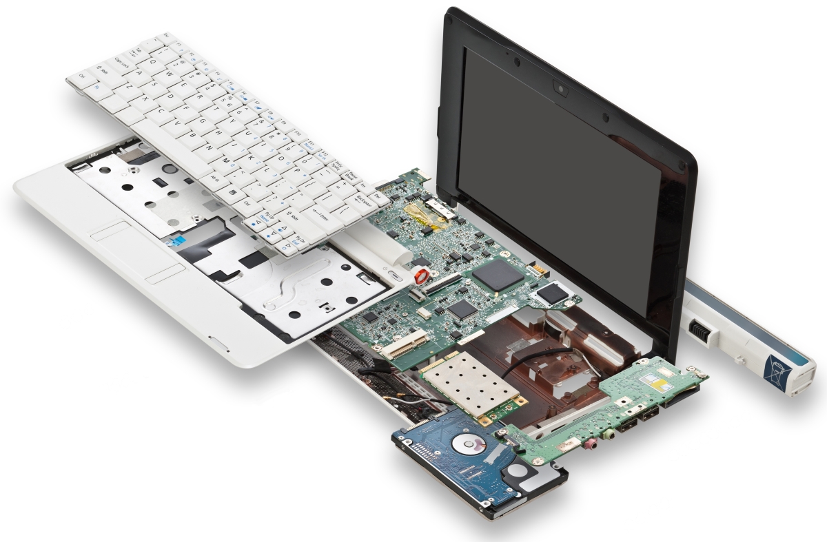
As a PCB Designer, I know that my field of work has morphed radically over the last two decades. Fresh out of school in the mid-1990’s, all of my early projects centered on either of two main areas: computers or computer peripherals. Sure, there was the odd stereo or clock radio, but 90% of the time I was working on a desktop motherboard or something close to it. This meant that, on an average day, my design efforts had a lot of real estate to work with. All on a two layer board, too. It was a different time. Thankfully, it didn’t stay like that forever.
Connection to the cloud is a key feature of the internet of things.
Fast forward to today, and I’m still designing PCB’s in the computer space. Big beige boxes aren’t the name of the game anymore - instead, it’s all about the Internet of Things (IoT). Through these embedded computers, a whole new category of gadgets and devices has opened up, especially those under the “smart home” moniker.
Coffee makers, kettles, refrigerators, lighting, watches, and even cars are all picking up this 21st-century technology. Integrating features like cloud control, remote access, and even machine learning (your air conditioner turns on as you commute back from work), it really is starting to feel like the future. Of course, for us PCB designers and electrical engineers, it means a lot more than party tricks and fuzzy logic toasters.
Internet of Things: More Complicated Than You Might Expect
For obvious reasons, building a PCB for an IoT device is a real challenge. Space, for instance, is at a premium. Most IoT products are small appliances, controls, or wearables directed at the consumer market, who like things neat and compact. Moreover, many of these devices are not designed with the hardware in mind. Instead, it’s all about the aesthetic, which means irregularly-shaped small spaces for hardware.
Then, there’s the matter of performance. No one’s going to be thrilled if their fridge needs to “load,” and if takes a lot of oomph to get that smartwatch to bring up YouTube. Your PCB will probably be packed with IC’s and at least one SoC, if not two. Finally, we need to consider reliability; consumers who buy these gadgets will expect them to “just work.” This means whatever design choices you make need to have rock solid foundations. There just isn’t room for error (or anything else for that matter) like there used to be. So then, what are the smart designers doing?
Smartwatches are a typical application of the Internet of Things. They require a lot of performance in a small package.
Flexible PCB’s: An IoT Project’s Best Friend
Allow me to share some personal experience with you. The simple two layer boards I reminisced about are a no-go. They just can’t do enough with small form factors. Now you’re probably thinking, “well what about high-density, multilayer boards?” Sure, that’s technically correct, but in my experience, they’re more trouble than they’re worth. With plenty of IoT products (especially wearables) on the move, those boards break too easily. Not only that, they need a flat space to fit in. There’s a better answer and it looks like everyone making IoT devices thinks so too. Flexible PCB’s have become the go-to in the IoT space, elevating a formerly obscure type of PCB to newfound prominence. Made from layers of polyimide, flexible PCB’s are capable of the same specifications of rigid circuit boards. They are widely adaptable without sacrificing long-term reliability and have demonstrated success in IoT applications. More importantly, their flexible nature lets them fit easily into the small and unconventional geometry of many IoT products.
On more than a few projects, I’ve been able to take advantage of the space behind curved faceplates and bases. I didn’t need as many connectors and ribbon cables either, and we all know how bulky they can be. Potentially, you could even create a common design that is able to fit within several IoT products of varying form factor (my boss loved that one). Flexible PCB’s and the IoT - it is a match made in heaven.
With so many companies big and small running after a piece of the IoT pie, you’ll probably be working on an IoT project in the near future. Naturally, if you’re as skeptical as I am, you might be apprehensive designing a Flexible PCB. Given the existing challenges associated with an IoT project, why would you want to make things more complicated? But much like the “chicken and egg” problem, the expanding IoT market has both improved and been enabled by flexible PCB’s.
About 8 years ago I can remember seeing some prototype flexible PCB’s while meeting a vendor, and they were admittedly very simple. Today, modern techniques like SMT, microvias, multi-layer substrates and BGA IC’s are readily applied. Thanks to better economy-of-scale, manufacturers can provide these features for cheaper. On the same budget, the range of design options on flex PCB’s has expanded dramatically. In fact, in a cost-benefit analysis, Rigid PCB’s are no longer an instant winner.
They’ve gotten stronger too, and as a result, possess greater reliability. There is, however, one thing that hasn’t changed, and that’s the design process itself. The workflow in your PCB CAD environment will be very similar: laying out traces, selecting and placing components, adding additional layers. On top of that, many recent design packages are bred to deal with flex designs and will give you insight on selecting dimensions and geometry. Honestly, even if you’re not totally “sold” on Flexible PCB’s, the landscape of PCB design will keep changing to make IoT happen. If they’re not good enough today, then they’re going to be great tomorrow.
As a fellow designer, I hope you’re as enthusiastic as I am working with flexible PCB’s. Both the technology and the design tools are much improved. Before you dive into the world of the IoT, it’s a good idea to take stock of the tools and resources at your disposal.
Flexible PCB’s have certainly transformed, but what about your PCB design package? Is it equipped to deal with the latest and greatest? Altium offers multiple solutions that scale to your needs while optimizing workflow.
Our professional PCB design packages are built to deal with the nuanced challenges of creating successful IoT products. With support for flexible PCB design, exhaustive testing tools, and an intuitive interface, Altium’s software is a reliable, trustworthy foundation for your next IoT project.


