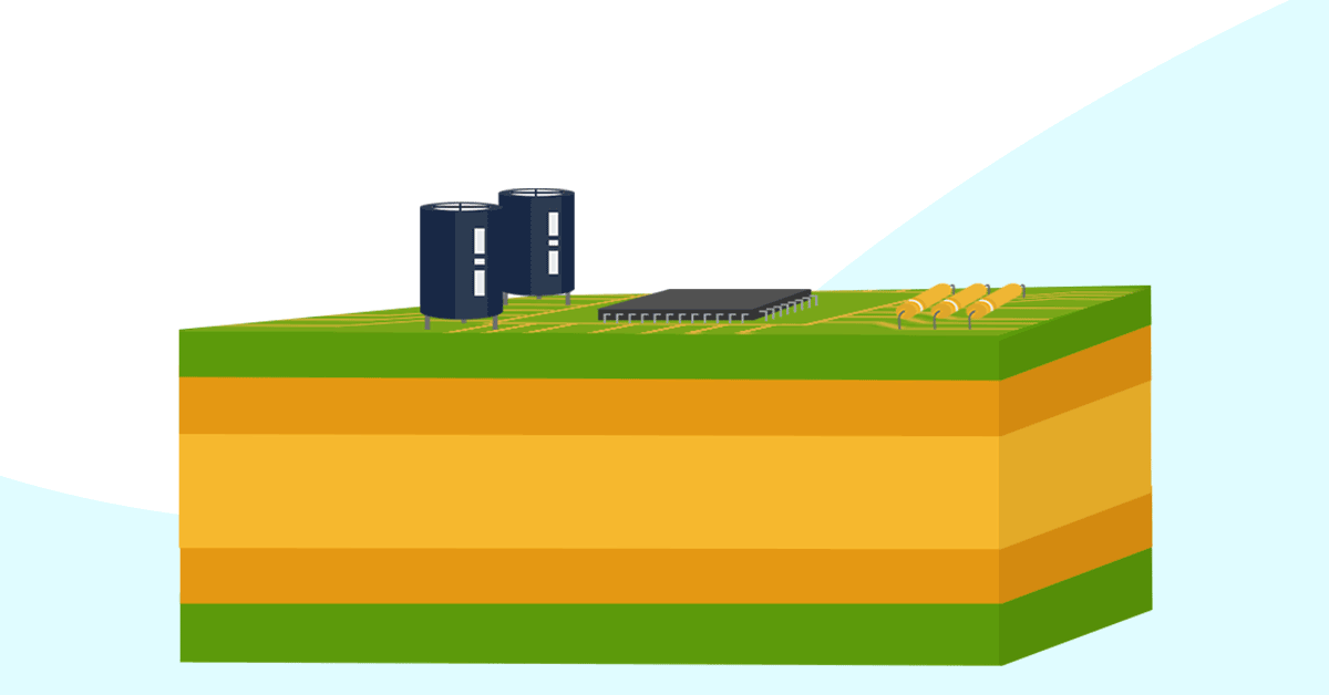
Understanding 2-Layer PCB Ground Planes

Table of Contents
Like many designers, my first board was a 2-layer board, and it didn't use a PCB ground plane. It wasn't very elaborate, just an amplifier with some connectors and a connection to a DAQ module that interfaced with a LabVIEW app. When you're designing with through-hole components on a copper-clad perfboard, there's no way to create a solid ground region anywhere on the board, and your grounding strategy will suffer for it. If you watch the upcoming podcast I had with Eric Bogatin, you'll note that he mentions that omitting a PCB ground plane in 2-layer PCBs is a common mistake among students and new designers. Today's designs, even if they aren't running at extremely high speeds, need to use a ground plane, something which is obvious to experienced design engineers but it confounding to newer designers.
In this guide, we want to look at how you should place and use a PCB ground plane, specifically in a 2-layer board. A digital ground plane design, even if done on a 2-layer board, may not need a specific impedance as defined by a PCB ground plane, but they will greatly benefit in terms of noise and ease of routing.
Does a Two-Layer PCB Need a Ground Plane?
In many situations, the simple answer is probably "yes". There are some situations where your device will at least work without a ground plane, but "working" and "success" aren't always the same thing. Placing your ground plane and routing to ground are two of the most important 2-layer PCB design rules and considerations. I believe the standard recommendation should be to always have a ground on PCB, even in a 2-layer design, unless you have a compelling reason to not use a ground plane and you've devised an alternative grounding strategy that can provide the connectivity you need. Doing this correctly creates a number of benefits that extend into multilayer designs.
Advantages of an Electronic Ground Plane in a 2-layer PCB
Using a PCB ground plane provides advantages in terms of signal integrity, power integrity, routing, and noise:
- EMI/EMC - Placing a ground plane below signals reduces their inductive susceptibility to EMI. In other words, it helps suppress crosstalk from inside the board and noise induced from sources outside the board. Placing a ground plane on the bottom layer of a two-layer PCB provides noise reduction; it reduces the loop area seen by signals.
- Stable switching - The grounded path followed by signals will have lower inductance, which helps create a lower inductance ground connection that reduces ground bounce. It will also be easier to place and route any caps needed for stable power.
- Solvability - It's easy to route back to ground in a 2-layer board with a ground plane; just drop a via and connect it directly to ground. You'll save a lot of space that would otherwise be used to route ground traces or rails.
In 2-layer boards, including dense boards that won't have the EMI/EMC and SI/PI problems I mentioned, using a 2 layer PCB ground plane is also preferable to just routing ground traces. Nearly every board that includes multiple components will simply not have enough room for routing return traces alongside all signal traces. Placing a PCB ground plane below the relevant components and signal traces also allows you to route ground returns directly from a component to the ground plane through a via. The return signal will then follow the path of least impedance back to the power supply return. This also allows you to easily place bypass/decoupling capacitors between power connections on critical components and the PCB ground plane, which allows any high frequency fluctuations in the power connection (e.g., conducted EMI from a switched power supply) from reaching the relevant components.

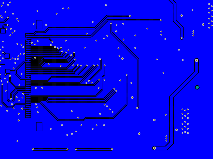
Beneath this simple looking RF design sits a ground plane.
When You Might Not Need a PCB Ground Plane
If you're developing a proof of concept or a prototype, and the design just needs to work decently, then you might be able to get away without a PCB ground plane as long as the design works with development boards and a breadboard setup. If you want to create something that will go to market, then you might have problems with excessive noise or radiated emissions if there is no ground plane on the PCB. In some layouts, it's just a lot easier to solve the design if you use a ground plane rather than a power plane. This is an important distinction and it's one of the reasons I try not to give "always/never" statements in this area: the design might function as intended, but that doesn't mean it will be low noise or commercializable.
That being said, there are a few instances where you can probably avoid using a PCB ground plane, and the design might function properly and have low emissions:
- The breadboard passes EMC - If the design passes EMC testing when laid out with modules, wires/cables, and dev boards. If the design has low enough noise that it will pass EMC in these conditions, then it will be very hard to make it worse once it's integrated onto a 2-layer PCB.
- DC only - With DC designs, you can usually do fine without a PCB ground plane as long as the system is not operating with high power or switching regulators. These designs might be susceptible to EMI, although this can be filtered to the point where it may be unnoticeable. Also the design will not experience the types of signal integrity and power integrity challenges seen in digital boards.
- Low density, tight coupling - When the board density is low enough, you can probably route a ground trace/rail alongside signals/power, and you can probably get away without using a PCB ground plane. If the design density is low enough and signal speeds are low enough, you might still pass EMC testing.
- All your signals are differential - Differential signals don't need ground for impedance and low differential-mode noise, although having ground doesn't hurt. Some example designs would be a digital interface converter module or an isolator module.
Gridding and Pouring Ground Regions
Since we're talking about 2-layer boards, one of the first points to consider in your design is real estate as you won't be routing signals through an internal signal layer. If your design limits your available space for components, then you might need to use an alternative grounding strategy instead of using a PCB ground plane. Rather than place a continuous ground plane across the entire bottom layer, there are two other possible techniques that can be used in a two-layer PCB.
The first option is to just use copper pour. This is a good option if you need controlled impedance (such as with USB); the impedance will be dominated by the presence of pour rather than the plane. If you can't fit an entire plane, you can at least fill in the board with copper and induce a return path in the pour. You would then just tie all the pour sections together with vias.
Another option you'll sometimes see described online is gridding on alternate layers. This involves placing two perpendicular grid patterns on both layers, and the grids can be connected with vias at points where the grids cross. This ensures that all sections of the grid remain at nearly the same potential and provides some extra real estate for components on both layers. A potential problem with this design is with routing between grids on a single layer. In this case, a grounded trace can be routed next to a signal trace, where the grounded trace is connected to the ground sections on the opposite layer with vias.
As with many 2-layer PCB design tips, gridding represents a tradeoff: you can create low inductance current loops with creative routing, but you might lose some of the EMI protection provided by a continuous ground plane. You also might not gain any new real estate on your board due to the grid. I've seen gridding recommend in a two layer board as an alternative to using a continuous ground plane on a single layer or using copper pour. For low speed/low frequency signals or DC boards, this may be just fine. However, in cases with high speed/high frequency without shielding or an environment with significant radiated EMI, you're better off with a 4-layer board with ground.
Mixed Signals? Be Careful With Sections in Your PCB Ground Plane
Some simple 2 layer PCB ground plane designs may still need to incorporate digital and analog signaling on the same board. One option is to use a star ground to separate the back layer a digital section and an analog section, but leave the two planes connected near the return to the power supply. This ensures that digital signals do not follow a return path beneath sensitive analog components. The key guideline here is:
- Do not route across any gap between plane sections. If you must have a signal cross between the two sections, just use a uniform ground plane, or use an optocoupler to cross the gap and maintain isolation.
Routing traces over a notch between the ground regions will create a very large return path for return signals in the PCB ground plane and is not recommended. These traces will radiate strongly and the circuit will have large loop inductance, leading to higher susceptibility to/generation of radiated EMI. It is also a bad idea to completely split a PCB ground plane in a 2-layer board and try to bring the sections to the same potential using something like a ferrite bead, as this creates more EMI and noise problems than it solves. This is especially true when you're trying to stitch disparate grounds together in a system with digital signals routed around the board.
When you need to design your PCB stackup and route your 2-layer circuit board, use the complete set of design features in Altium Designer®. When you’ve finished your design, and you want to release files to your manufacturer, the Altium 365™ platform makes it easy to collaborate and share your projects.
We have only scratched the surface of what’s possible with Altium Designer on Altium 365. Start your free trial of Altium Designer + Altium 365 today.
Check out Altium Designer in action...
Powerful PCB Design

About Author
Related Resources


Related Technical Documentation


Take advantage of the world's
most trusted PCB design system.
One interface. One data
model. Endless possibilities.
Effortlessly collaborate with
mechanical designers.
The world's most trusted
PCB design platform
Best in class interactive
routing
View License Options
Thank you, you are now subscribed to updates.