PCB Design Verification Datasheet

Table of Contents
TOPICS IN THIS SOLUTION
FEATURES AND BENEFITS
- Validate your design with XSpice before you even start laying out the board to expedite layout and prevent errors
- Identify power distribution network issues during the design phase
- Running the right simulation ensures your board will meet the design requirements
DESIGN VERIFICATION
Sometimes you are not sure how a design verification will behave or maybe you just want to explore a few design process ideas before committing to manufacture. The true mixed-signal simulator in Altium Designer® helps you verify and tune your design validation concepts quickly and accurately. Altium Designer allows you to easily create and manage multiple simulation profiles. Separate profiles allow designers to run different types of analyses and design reviews or durability testing with different simulation engines (Mixed Sim, SIMetrix, SIMPLIS). This allows for multiple runs of the same simulation type (e.g., AC analysis) with different parameters and options (e.g., different frequency ranges). Active profiles can easily add, remove, edit, run, and/or generate netlists. The profile manager organizes profiles and uses probes or active nets to select waveforms to display. All simulation results can be saved with other manufacturing outputs for conveyance to manufacturing.
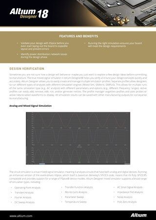
Analog and Mixed Signal Simulation

Analog and Mixed Signal Simulation
The circuit simulator is a true mixed-signal simulator, meaning it analyzes circuits that have both analog and digital devices. Running an enhanced version of the event-driven XSpice, which itself is based on Berkeley’s SPICE3 code, means that it’s fully SPICE3f5 compatible and provides support for a range of PSpice® device models. Altium Designer mixed simulator supports a broad range of simulation types, including:
- Operating Point Analysis
- Transient Analysis
- Fourier Analysis
- DC Sweep Analysis
- Transfer Function Analysis
- Monte Carlo Analysis
- Parameter Sweep
- Temperature Sweep
- AC Small Signal Analysis
- Impedance Plot Analysis
- Noise Analysis
- Pole-Zero Analysis
Simulation Profiles and Probe Management

Flexibility to Select Circuit Simulation Probe Source Data and Waveform Measurement Types
With the probe manager, you can display plots from your design review without needing to manually add or modify waves post simulation. This added flexibility and control saves what matters most: time. Within the development of the probe manager you’re able to view and manage which probes are enabled or disabled for respective product simulation device profiles. By being able to toggle product simulation profiles on or off, you’re able to clearly display only the profiles you’re interested in.
PDN Analyzer

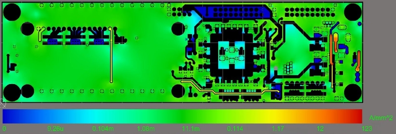
2D Current Density PDN Analysis Results: note the hot spots on the right that need further attention
The challenges of designing power distribution networks (PDN) for modern high-speed electronics are a constant development test factor for design professionals. These challenges stem primarily from the simple fact that switching speeds are continually increasing, leading to drops in supply voltages while current requirements creep upward. The Altium Designer PDN Analyzer™ extension, powered by CST™, addresses these issues to help designers foresee and correct any potential PDN issues early in the design validation phase. It provides an integrated, inexpensive tool that is easy to learn and set up so that designers can visually emulate their designs power circuits early on during the design process. Once the simulation has been run, the resulting analysis data, consisting of voltage and current density, is graphically modeled in the PCB editor as a rendered 2D or 3D image.
Looking for more information about Design Verification? Reach out to our support team, or call our toll free phone number at 1-800-488-0681 today.
 Open as PDF


