Build Your Own Patch Antenna for Your Next PCB

Table of Contents
Patch antennas are one of the simplest to design and they offer a simple polarized emission solution, especially at high frequencies. They can also be probe-fed, which is something you might find in an external patch antenna module connected via a coaxial probe. To design a patch antenna, only a few simple formulas are required, and it's possible to design probe-feeding into the antenna to operate as an external module.
This article primarily provides the design equations for patch antennas in a PCB. At the end of the article, I'll provide a link to a calculator that can be used to get much more detail on a patch antenna, including a feedline matching method.
Patch Antennas on a PCB
Patch antennas are simple to design on the surface layer of a PCB and they obey two simple design rules:
- Patch antennas are placed over a ground plane, and the ground plane should extend well beyond the edges of the antenna
- The width of a patch antenna is sized to support a standing wave resonance between the patch and the ground plane
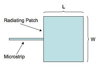
Ideally, patch antennas in a PCB should be placed close to the ground plane, so they are best used in 4-layer boards with the ground plane on an inner layer. For example, if the antenna is on L1, then GND should be on L2. All patch antennas operate as leaky resonators, where radiation is emitted from the surface and edges of the antenna structure. The image below shows the basic structure of a patch antenna with its feedline placement along the width direction.
The field line distribution for the fundamental mode between the patch and the ground plane is shown below. The fundamental mode is the TM10 mode (transverse magnetic), and the feedline is placed to ensure excitation of this fundamental mode. This placement will also determine the input impedance looking into the antenna, which is discussed more below.
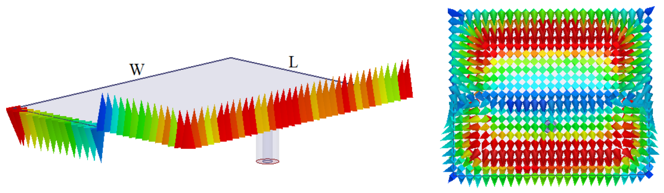
This field distribution in the fundamental mode determines the radiation pattern around the patch antenna. The design equations that will be shown below are based on this operation in the fundamental mode.
One of the challenges with a patch antenna placed on a PCB is that they can be rather large. The fundamental mode will have the largest operating wavelength, so this will determine the overall size of the patch antenna. Using a substrate with a larger dielectric constant will allow the patch antenna to be made smaller if required. At lower frequencies, such as WiFi or lower, patch antennas may not be the best choice on a PCB due to their size. However, at much higher frequencies in the mmWave range, patch antennas are very useful due to their ease of design and their small size at high frequencies.
Patch Antenna Radiation Pattern
Patch antennas exhibit omnidirectional emission above the patch region, or rather above the ground plane in the PCB. The emission is very poorly confined along the surface of the PCB and instead has a nearly spherical distribution in the far field. Therefore, patch antennas in a PCB make useful omnidirectional radiators. The image below shows a radiation pattern from a patch antenna operating at 2.45 GHz (simulated in HFSS).

The radiation pattern shown above appears nearly isotropic, but notice that the peak gain is much larger than 0 dBi (peak of 4.2797 dBi). The peak gain of a patch antenna can tend towards +9 dBi, depending on the substrate thickness, dielectric properties, and span of the ground plane beneath the patch antenna. Conceptually, this occurs because the ground plane beneath the antenna does reflect radiation away from the PCB and into free space. Reflection from the ground plane allows for superposition of radiation around the patch antenna, and this creates the non-isotropic radiation pattern given above.
Patch Antenna Design Equations
The following set of equations can be used to design a patch antenna on a PCB. The only required inputs are the PCB laminate material dielectric constant, the layer thickness, and the frequency of operation. There will be an effective dielectric constant that determines the requried length of the patch antenna, as well as the relation between geometry and operating frequency.
To start, select an operating frequency and dielectric constant for the PCB substrate material, and calculate the required width of the patch antenna.

Next, use this value to calculate the effective dielectric constant using the thickness of the PCB laminate (distance to the ground plane:

Finally, use the above results to calculate the required length of the patch antenna:

The impedance of the resulting antenna design will be the ratio of the electric and magnetic fields (technically it is a wave impedance). This means that the impedance varies along the edge of the antennna, and it will vary with the PCB laminate properties (thickness and Dk value). To determine the impedance, scroll to the end of this article and find a link to our patch antenna calculator page. That page includes a formula for the TM10 mode impedance and a calculator that will give the impedance and bandwidth.
Higher Order Modes
As was mentioned above, the standard implementation of a rectangular patch antenna in a PCB will operate in the TM10 mode. For any resonator, there will be an infinite number of modes that produce standing wave resonances, which can then emit into space around the antenna structure. These higher order modes can be excited directly when an input signal matches the resonant frequency of the structure. The frequencies for the higher order modes are given by:

Note that the L* term refers to L above, plus the 2nd term on the right hand side. In the TM10 mode refers to the i = 1 mode (j = k = 0). The effective Dk value used in this frequency equation is the same as that used in the above desgin equations. This is the lowest-order mode that can be excited when the feedline is routed into the edge.
Feeding Methods: Direct, Coaxial, and Inset
In order to excite a patch antenna, or to collect the signal received by a patch antenna, the antenna will need a feeding method. There are three often-cited methods for applying a feedline:
- Direct connection between a microstrip and the antenna with a quarter-wave transformer
- Placing an inset for a microstrip feedline into the antenna
- Connecting a coaxial probe into the antenna on the back side of the antenna
These three methods are outlined in the image below.
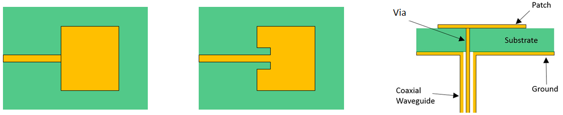
Direct connect - The direct connection method simply involves transforming the antenna's input impedance to a different value using a impedance transformer. Technically, any impedance transformer could be used, or an LC network could be used to match the impedance of the microstrip feedline to the patch antenna. The most commonly cited method is to use a quarter wavelength transformer because the design formula for this transformer is very simple.
Inset feedline - The inset method involves setting the microstrip connection point slightly into the interior region of the patch antenna. This is a useful method because it allows the impedance transformer in the direct connect method to be eliminated. Instead, the input impedance of the antenna is matched directly to the microstrip line's impedance. By eliminating the matching sections, you can reduce the overall size of the antenna and its feedline sections.
Coaxial probe - The coaxial probe method may be used for routing into a patch antenna that is placed on an external module; a standard SMD coaxial connector could be used on the back side of a PCB to make this connection. The coaxial connection can be made through a via into the patch, but the via entry will not be into the center of the patch when the patch is operating in the fundamental mode. Instead, it will be slightly off-center. The placement here is determined by impedance matching the coaxial line input to the input impedance of the antenna at the feedline point. In higher frequency systems, the feedline input impedane will be dominated by the via impedance.
One other possibility is to use a trace taper to interface with a patch antenna. However, the design rules for a trace taper on a microstrip feedline into an antenna may require empirical equations that are not easily generalized. The design approach used with a trace taper routed into a substrate integrated waveguide can also be used with a patch antenna as long as the fields at the input edge are known.
More Resources for Patch Antenna Design
Simpler patch antennas with rectangular shape are easy to design with the above formulas, and the above patch antenna designs can be cascaded into circular and parallel arrangements. There are more complex types of patch antennas and arrangements that can be designed on a PCB. Some of these include:
- Series and parallel arrangements of patch antennas
- Aperture-fed patch antennas
- Notched patch antennas that provide controlled polarization
- Circular patch antennas (see below)
- Fractal patch antennas
- Circularly-polarized patch antennas
To help designers build rectuangular patch antennas operating in the fundamental mode, we created a microstrip patch antenna calculator that is free to access. It will calculate the size, impedance, and bandwidth of a patch antenna:
Patch antennas can also be circular or elliptical for a given operating frequency. In the circular case, instead of the operating frequencies being related to rectangular resonances, they will be related to circular resonances defined by cylindrical Bessel functions. For more general patch antenna designs, the field distribution, radiation pattern, input impedance, and polarization characteristics all need to be computed with a field solver as they may be difficult to determine from analytical formulas. HFSS is the most useful tool for this, and you can use the Ansys EDB Exporter extension in Altium Designer to access this utility for patch antenna design.
The CAD features in Altium Designer® are ideal for any type of design you want to create, ranging from high-speed digital PCBs to advanced RF systems. When you’ve finished your design, and you want to release files to your manufacturer, the Altium 365™ platform makes it easy to collaborate and share your projects. Come see the newest feature releases in Altium Designer.
We have only scratched the surface of what’s possible with Altium Designer on Altium 365. Start your free trial of Altium Designer + Altium 365 today.

About Author
Related Resources


Related Technical Documentation


Take advantage of the world's
most trusted PCB design system.
One interface. One data
model. Endless possibilities.
Effortlessly collaborate with
mechanical designers.
The world's most trusted
PCB design platform
Best in class interactive
routing
View License Options
Thank you, you are now subscribed to updates.