PCB Design Guidelines for Using TVS Diode for Transient Protection

Table of Contents
For hardware engineers, surge protection is about more than buying the right power strip or unplugging a couple of cables. It involves strategically placing transient protection components in the PCB layout and implementing a clear grounding strategy. TVS diodes are a common component used to protect components in a PCB layout. These components are placed on data lines and they operate by diverting current away from a protected component once an ESD pulse is received in the circuit. Ensuring that your PCB layout is optimized for transient protection can mean the difference between a functional device and a fried circuit board.
What is a TVS Diode and How Does it Work?
A transient voltage suppression (TVS) diode is a component that is commonly used to protect a device against transient events associated with electrostatic discharge (ESD). (Not to be confused with zener diode or schottky diode.) It consists of a p-n semiconductor junction that becomes conductive during a transient voltage spike. In normal circumstances, a TVS diode has high impedance with very low leakage current, effectively acting like an open circuit.
When the voltage on the transient voltage suppressor rises across its threshold voltage, the avalanche effect in the semiconductor causes the p-n junction to begin conducting, providing a low-impedance path that channels the excessive current away from a protected device. The response time of the TVS diode is extremely fast, often expressed in picoseconds, so these components can very quickly divert a strong ESD pulse, even if that ESD pulse has a relatively fast rise time.
Choosing the Right TVS Diode for Your Design
All TVS diodes are basically diodes: if you apply a large enough forward or reverse bias voltage, they will begin to conduct. Of course, not all TVS diodes are created the same. Choosing the wrong one for your design may render the transient protection ineffective from the start. There are a few parameters that you’ll need to understand when choosing a TVS Diode:
- Reverse Bias Breakdown Voltage (VB) - This is the reverse bias voltage at which the TVS diode will start conducting. Once the TVS diode starts conducting, it will divert the ESD pulse away from the protected component.
- Clamping Voltage (VC) - The clamping voltage is the minimum voltage at which the TVS diode will conduct significantly after reverse bias breakdown is exceeded. This value is defined within the limit of the specified peak current. In general, a lower VC value will provide more protection to a component, and VC should be selected so that it is less than the input voltage limit of the protected component.
- Rated Standoff Voltage (VWM) - This indicates the reverse bias voltage limit below which the TVS diode will remain insulating. Within the Rated Standoff Voltage, the TVS diode has a high impedance with only a small amount of leakage current.
- Peak Pulse Power Dissipation (PPP) - The TVS diode needs to be able to safely dissipate the excessive current caused by the transient voltage. This is indicated by the Peak Pulse Power Dissipation.
How Does a TVS Diode Work?
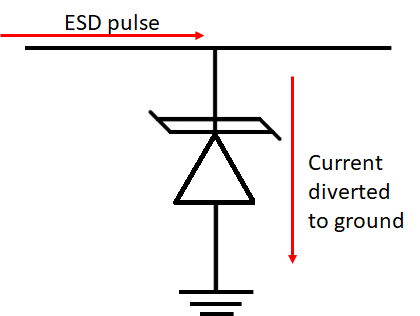
All TVS diodes work on a simple principle: when an ESD pulse is received on a circuit, the pulse can very quickly exceed the reverse bias breakdown voltage value for the diode. Devices that expose any of their conductors to the external environment, such as through a connector, can receive ESD pulses on those conductors. If those conductors are part of a signal line leading to a compoent, the received ESD pulse will transfer a high-voltage/high-current pulse into the component. This could destroy the component.
When ESD occurs on a signal line and a TVS diode is present on the signal line, the diode will begin conducting and the pulse can pass through the diode. This allows the diode to divert the ESD pulse away from the protected circuit. The typical connection is to connect the anode to a ground connection, so the ESD pulse will be passed into ground. As long as there is a low-impedance path in the ground region, then the pulse will be diverted away from the protected component.
Bidirectional or Unidirectional?
TVS diodes come in two varieties: bidirectional and unidirectional. These two types of TVS diodes have different symbols as shown below.
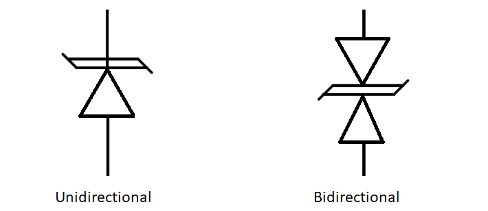
When shopping for TVS diodes, it's important to note that the blanket term "TVS diode" only refers to the unidirectional type. So if you need a bidirectional component, you need to make sure this is specified.
So which type of TVS diode should you choose? The main reason to use a bidirectional TVS diode is to provide protection when the circuit is carrying positive and negative polarity signals. This is why you might see bidirectional TVS diodes on a differential pair, or on an analog line that oscillates between positive and negative polarity.
I'm a firm believer that you should prefer a bidirectional TVS diode for comprehensive fault protection and ESD protection. This is because the ground region can receive ESD pulses, just like the signal lines you want to protect. If there is a ground fault that causes the path through ground to have high impedance, then the lowest impedance path might be through a unidirectional diode and through the component you want to protect! However, if the diode is bidirectional, it has a chance of still protecting the component even if there is a ground fault.
PCB Layout Tips for TVS Diode
Besides choosing the right TVS diode, the effectiveness of the protection is determined by the PCB layout itself. An example bidirectional TVS didoe is connected in parallel to the circuit that it is protecting in the schematic below. The schematic indicates a typical connection of a TVS diode to a MAX3485 transceiver:

Schematic of typical of TVS Diode connection.
In this example, if an ESD event were to occur where the D+ and D- lines are exposed to the external environment, and this event created a positive voltage with respect to GND, then the TVS diode would begin conducting as long as the ESD voltage exceeded the TVS reverse bias breakdown voltage. If there was an ESD event that caused current to begin flowing in the GND plane, the current should be totally diverted away from the components as long as there is a low-impedance ground path in the system.
In the case where ESD is received by the ground conductor, a bidirectional TVS diode is preferrable because it will still offer some protection, whereas the transceiver might still be exposed to some voltage if the TVS diode was unidirectional. The preferrable diversion with the bidirectional TVS diode occurs because the applied pulse would need to rise above some threshold (the VB value for the top half of the TVS diode) before conduction can occur from GND to the traces.
In a PCB layout, a few important guidelines should be followed for TVS diodes to function correctly. These include placement, grounding, and use of any passives like resistors or capacitors on shielding.
Placement of TVS Diodes
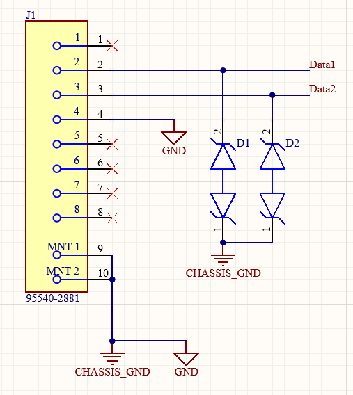
Because ESD can occur near exposed conductors in an electronic device, it's best to put TVS diodes near the region where those conductors are exposed to the external environment. A simple layout example with a 2-pin connector is shown below.
Place TVS diodes near exposed conductors that are in danger of recieving an ESD pulse.
PCB traces have some parasitic inductance that may cause the clamping voltage of the TVS diode to increase above its specified limit. The trace of the TVS diode should also be comparatively short to the trace of the transceiver to minimize the impedance and ensure that the excessive energy in the surge is dissipated. This will minimize the parasitic inductance in the path leading to the TVS diode.
Grounding
If possible, it's a good idea to connect the TVS diode to a different ground net than the protected component. This does not mean you should split ground planes. Instead, the safest type of connection is to have the TVS diode connected to metal element in a chassis ground if it is available, with the connection normally being made with a trace connected to a chassis screw or a mounting hole. If this connection is not available, then the connection can be made to an internal plane. However, in an environment where there is risk of strong ESD, the device should be packaged in a chassis that has a safe metallic chassis ground followed by an earth connection.
Eliminate Passives on Shielding
Some components like shielded connectors will have some additional metal shielding that protects the exposed conductors. Shielding on connectors is not meant for mechanical or thermal protection, it is actually meant for preventing noise reception and protecting against ESD. If there is some danger of ESD, then shielded connectors can be used alongside TVS diodes. The TVS diodes are connected to the signal lines, and the shielding on the connector is connected directly to ground.
In the above image, I've placed a direct connection between chassis and signal grounds. The typical approach is to put this connection at one location in the system so that you ensure uniform ground potential on all conductors, but you still control regular return currents so that they do not pass through the chassis. I would say the same applies here as long as GND is a low-impedance, low-inductance ground plane. If this were a galvanically isolated region of the system, it might be best to put that connection closer to the connector body, as is implied in the above schematic.
There are some cases where you will see someone try to connect the shielding to ground through a snubber circuit or a parallel RC circuit. Both of these defeat the entire purpose of having a shielded connector. Instead, make a direct connection between the shielding and chassis ground (if available) or to the ground plane. This will create a very low impedance path to ground that prevents energy in an ESD event from reaching a protected component. In some cases, where there will be trouble controlling return currents (such as with a floating ground), the appropriate approach is to put a large capacitor between the shield and ground plane; this ensures fast ESD pulses can be shunted and there will not be high-frequency noise radiated from the system due to any offset between the two grounds.
When you need to create components, capture schematics, create your PCB layout, and place TVS diodes for circuit protection, look to the complete set of PCB design features in Altium Designer®. As you build your schematics and select TVS diodes, you'll be able to implement the PCB layout and grounding techniques outlined here to ensure protection of important components from ESD. When you’ve finished your design, and you want to release files to your manufacturer, the Altium 365™ platform makes it easy to collaborate and share your projects.
We have only scratched the surface of what’s possible with Altium Designer on Altium 365. Start your free trial of Altium Designer + Altium 365 today.

About Author
Related Resources


Related Technical Documentation


Take advantage of the world's
most trusted PCB design system.
One interface. One data
model. Endless possibilities.
Effortlessly collaborate with
mechanical designers.
The world's most trusted
PCB design platform
Best in class interactive
routing
View License Options
Thank you, you are now subscribed to updates.