Pulsed Laser Diode Driver Circuit Layout for Lidar
Table of Contents

As part of the sensor suite for autonomous vehicles, lidar range maps play an important role in object identification in the surrounding environment, alongside car radar and other sensors or imaging systems. Building a functional driver circuit with small form factor and sleek packaging is critical for enabling lidar imaging/rangefinding around a self-driving vehicle.
These same circuits can be adapted to other lidar applications, such as atmospheric monitoring, pollution plume tracking, turbulence measurements in aircraft, and other precise measurements. The primary factors that determine the usefulness of your particular lidar system are the power output, pulse time, and repetition rate. If you design the right driver circuit, or properly adapt your diode to a driving IC, you can ensure that your lidar system will operate with high resolution and range.
Driving a Pulsed Laser Diode - The Transmit Side
Pulsed laser diodes are driven with high voltage, low duty cycle PWM pulses (usually ~1% duty cycle at hundreds of kHz) in order to reach 100 ns or faster pulse widths. Driving a pulsed laser diode with a smaller rise time provides higher resolution images and allows for a faster scanning rate. The short rise times required in driver ICs and in custom circuits requires use of GaAs devices for longer pulses, while GaN is the best choice for shorter pulses.
If you’re designing your own driver circuit, the critical components are the FET driver and transmit amplifier stages. The signal to drive the pulsed laser diode is initially amplified with an FET driver, which then switches on a high current FET transimpedance amplifier with high gain to deliver the required drive current. A block diagram of this circuit is shown below.
Pulsed laser diode driver circuit block diagram
This circuit is designed to be a current-mode pulse driver circuit. Remember, current-controlled devices like LEDs or laser diodes have low impedance above their rated forward voltage; the driver circuit is acting as a current source that needs to drop all of its power over a low impedance load. Since this is basically a pulsing power amplifier, you need to ensure the voltage dropped across the laser diode does not exceed the compliance voltage.
However you choose to drive your pulsed laser diode, you’ll need to ensure the jitter in the output is very low. This is critical because, when you’re working with signals that travel at the speed of light, jitter of 1 ns equates to a distance error of 30 cm. You’ll need to bring that jitter down by a factor ~10 to ensure accurate distance measurements. Reduction of jitter typically focuses in three areas: power, impedance, and parasitics.
Low-inductance Power Paths
A simplified example of a capacitive pulsed current drive with a single MOSFET switching element is shown below. In this topology, the FET should be chosen so that it can be switched with logic levels, yet it should have minimal parasitics where possible to prevent distortion of the desired pulse. Stable power delivery at the required pulse rise time and shape relies on maintaining low impedance throughout the PDN/signal chain leading to the laser diode (marked "LD" below).
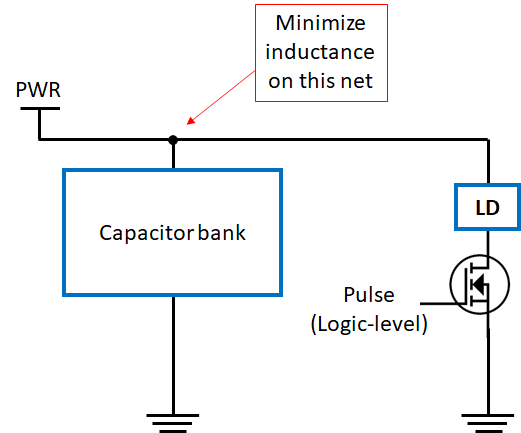
While this topology might seem very basic, component selection and layout are the main challenges. All the components must be carefully selected as parasitics in the components and the layout will combine to determine the pulse shape, as well as problems like ringing or excessive noise. This includes inductance on all component leads, the PCB traces, and planes. More common is to replace the FET with an amplifier; make sure the amplifier feedback loop has minimal inductance to prevent ringing, otherwise you may see this superimposed on the light output from the laser diode.
Do You Need Impedance Matching?
This question relates to jitter and the behavior of a laser diode as a nonlinear load component. If you're familiar with nonlinear signal chains, maximum power transfer between a power amplifier (running near saturation) and a nonlinear load will typically occur when there is some slight impedance mismatch. The exact amount of impedance mismatch is determined using a technique called load-pull analysis.
To get to the perfect amount of impedance matching, in series with the laser diode, you would need to layout an impedance matching circuit. Unfortunately, this can add new parasitic inductance that create the potential for an underdamped oscillation in the amplifier circuit. Instead, we only worry about low-impedance current delivery by appropriately designing the PDN and selecting an amplifier/FET that provides the required low output impedance, rather than trying to transform the input impedance to a different value.
The Receive Side
On the receive side, the reflected/scattered lidar pulse is received with a photodiode array or other detector, and the received signal is used for a time-of-flight measurement, which can easily be performed with time-to-digital converter ICs. Afterwards, the received signal at each emission angle is sent to an ADC and is used to build a depth map from the time-of-flight measurements. On the receiver side, a time-of-flight measurement is performed in two ways:
- By applying low-frequency modulation to the driver and measuring the phase difference between driven and received modulated pulse streams
- By directly measuring the time between the arrival of pulses (usually with ~100 ps resolution)
Because jitter adds in quadrature, you’ll need to remove jitter before the amplification stages on the transmit and receive sides. Pulsed laser diode driver ICs typically include a fractional PLL that converts a reference clock to match the scanning rate in the system. This converted clock signal is then used on the receive side for time-of-flight measurements and for serializing output data from the ADC.
Pulsed vs. CW
Note that we’ve focused on pulsed laser diode driver circuit layout here, but a continuous wave (CW) laser can be operated as a pulsed laser. However, if you intend to drive a CW laser diode as a pulsed laser diode, you should gather an an autocorrelation measurement to determine the pulse width, which is difficult without sensitive optical equipment and a fine mechanical delay stage. Modulated CW lasers will have lower output power and may be more difficult to detect in a time-of-flight measurement. Therefore, don't get any bright ideas and just stick with pulses.
Temperature Control
Finally, the output power from a laser diode and the sensitivity of the detector on the receive side are sensitive to temperature. In general, the efficiency of a laser diode and sensitivity of the detector both decrease at higher temperature. A temperature increase of both components is inevitable during operation, requiring a creative thermal management strategy. This might include a small cooling fan, but in my opinion, a better choice is to use a high thermal conductivity heat sink or substrate and try to dissipate heat to the enclosure as this uses fewer moving parts.
Use Your MCAD Tools
Any optical system carries precise mechanical tolerances, and pulsed laser diodes for lidar systems are no different. Lidar systems for autonomous vehicles will need to rotate around the entirety of a vehicle to provide depth images of the entire surrounding environment. Other systems can remain static, but they still require precise positioning with respect to any other optical components in these systems. During the layout phase, you should use your MCAD tools to verify precise positioning on the board and in your enclosure.
With the powerful PCB design and analysis tools in Altium Designer®, you’ll have a complete electromechanical design solution that is ideal for building optical and optoelectronic systems. You’ll also have access to signal integrity tools that can help you address impedance matching between your pulsed laser diode driver circuit and your diode.
Now you can download a free trial of Altium Designer and learn more about the industry’s best layout, simulation, and production planning tools. Talk to an Altium expert today to learn more.

About Author
Related Resources


Related Technical Documentation


Take advantage of the world's
most trusted PCB design system.
One interface. One data
model. Endless possibilities.
Effortlessly collaborate with
mechanical designers.
The world's most trusted
PCB design platform
Best in class interactive
routing
View License Options
Thank you, you are now subscribed to updates.