Simulation Driven Design Can Solve Your PCB’s Signal Problems and More

Table of Contents
If you work in the electronics industry or in research, there’s a chance that simulations are a regular part of life. Simpler systems can be designed with intuition and simulated after designs are completed, but more advanced systems running at high frequencies or very high data rates need qualification before and after a PCB layout is complete. Simulation software has to take a more prominent role in PCB design for many advanced systems.
Unfortunately, many simulation tools are not so intuitive for most designers as they were not built for use by PCB design software users. The tide is turning and these systems are getting much better in terms of usability, but their use within the design process is what makes simulation tools so powerful.
What to Examine in PCB Simulations
Simulation-driven design for electronics starts by creating an interface between your design tools, data management system, and simulation applications. Today’s professional electronics design teams are multifunctional with experience spanning across electrical, mechanical, thermal, and reliability disciplines. Design teams need systems that help them quickly share physical design data, export simulation models, and run design evaluation simulations.
The simulation-driven design process for PCBs spans three broad areas and follows a particular process:
- Circuit simulations
- Board-level simulations
- Assembly simulations

The process is iterative, which is why I draw arrows pointing back to previous steps. Any problem identified in circuit simulation results can force you to go back into the schematics and modify yout circuit designs. At the PCB simulation stage, the results may indicate required modifications in the circuitry, PCB layout, or both. This can be the case with EMI simulations, SI/PI, and thermal simulations; all of these results may indicate required changes in your circuits, which can then force you to make changes in the PCB layout.
Circuit Simulations (Including Transmission Lines!)
SPICE users know all about circuit simulations. A huge range of important behavior can be examined and evaluated in SPICE simulations, both in the time domain and in the frequency domain. SPICE simulations are the mainstay of circuit designers, and the basic
- Determine whether analog and power circuits provide intended functionality
- Use power expectations in circuits for later simulations
- Verify component tolerances on precision circuits
- Verify specialty logic functionality in a phenomenological logic circuit
All of these tasks can be performed in SPICE simulations as long as model definitions for components are available. Any of the above listed areas could take up space for its own article, so I won't go into those points here.
Systems that require digital signal integrity or RF signal simulations at the circuit or schematic level tend to be much more advanced and they require an equivalent circuit model or linear network defining the behavior of that structure. Simulations with these structures in your circuits use network parameters, typically ABCD parameters or another linear network parameter set that allows simple cascading between linear components.
- Design a candidate transmission line or RF structure on your intended stackup
- Simulate its performance, typically using S-parameters or transfer functions
- Iterate the design to maximize performance targets
- Once performance is acceptable, extract a linear network model or equivalent circuit model
- Use the extracted model in your SPICE simulations with your other components
Linear network models for these structures can be extracted with a simulation program like Keysight PathWave ADS, Simbeor, Ansys, or CST Microwave. An example extracted linear network determined from a package design on a PCB is shown below.
Extracted linear network for two component packages and their interconnect on a PCB. Image courtesy of Simberian.
Once this linear network or equivalent extracted circuit is brought into your circuit simulator, you can simulate the performance of your intended interconnect design. This type of simulation process is a standard approach used to understand behavior of interconnects on fast digital buses, such as DDR, PCIe, MIPI standards, etc. Once the intended design is qualified, you can use this in your PCB layout along with your other components.
Circuit simulations assume a perfect world, where a circuit is isolated from all other circuits. Real effects involving noise, signal coupling/crosstalk, and radiated/conducted emissions need to be determined at the PCB level once the layout is finished.
Board-level Simulations
Once the PCB layout is complete, board-level simulations are performed to evaluate important interconnects, power, EMI/EMC, and temperature. Not all parts of the PCB need to be simulated; the most important circuits that were examined in circuit simulations should also be examined in post-layout simulations where possible. For example, this could include:
- Signal integrity: MoM/BEM simulations for impedance verification and network parameter extraction, BER simulations in high speed channels, reflection and crosstalk waveforms
- Power integrity: PDN impedance extraction, transient modeling, current density mapping, with scanning from DC to GHz frequencies
- EMI analysis: Near-field and far-field radiation from high-speed/high-frequency interconnects, EMI from transients, shielding effectiveness, and EMI susceptibility can be examined
- Thermal simulations: Temperature distribution due to Joule heating from high power components and heat from external sources, natural and forced convection, thermal conductivity mapping
The list of specific board-level simulations that could be performed is quite long, but the goals are always the same: ensure that the placement of parts and interconnect designs in the PCB layout does not affect the performance of your system as it was qualified in circuit simulations. It's important to compare the pre-layout and post-layout results to ensure the device is not greatly affected by the elements placed into the PCB layout.
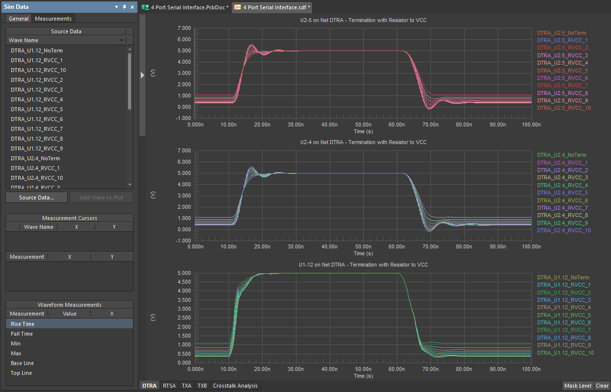
Much of the time, this relates to signal integrity, and this area of design typically receives major focus. Here are can example simulation results that you can generate from your Altium PCB layout:
- Identifying Near-field EMI in a PCB's Power Distribution Network
- Analyzing Crosstalk on FIFO and DDR4 Parallel Bus Interfaces
- Spotting DDR4 Impedance Violations in High Speed PCB Design
Eye diagram comparisons, S-parameter simulations, and impedance calculations are some of the main tools used to qualify interconnects for digital signal integrity.
Other areas where post-layout simulations are very important at the PCB level are power integrity and thermal integrity, both of which relate to functionality and reliability, respectively. However, things can change yet again once the design is put into its completed assmbly and intended enclosure/packaging. This is where collaboration with another group of simulation engineers is needed to qualify mechanical and thermal performance, as well as potential for EMC failure.
Assembly Simulations
Once the board is fully assembled, the thermal demands can change somewhat, and the board may need to be qualified mechanically to ensure its reliability, ability to withstand shocks, or ability to withstand vibration. These are just a few examples of the mechanical points to examine in a completed assembly.
- Mechanical simulations: Stress distribution leading to failure due to mechanical shock, bending, vibration, drop tests
- Reliability and lifetime: Failure probability due to thermal cycling, thermal/mechanical shock, moisture ingress, and vibration fatigue; evaluation against industry reliability standards
- Airflow and heat dissipation: In the enclosure, airflow typically must follow a specific path, and the enclosure can impact heat flow away from the core parts of the device
These aspects of qualifying an assembly are performed using more advanced field solvers and they do not directly involve your PCB design and layout software. The PCB design tool you use should provide a compatible mechanical or electro-mechanical export file that can be used in your field solver application.
For airflow simulations, a CFD-thermal co-simulation application is needed, and this is typically performed by a multiphysics specialist. An example involving the completed assmbly, complete with
EMI/EMC will also be affected by the presence of an enclosure and mechanical elements in the product, so it is worth simulating these points as well. This again involves a 3D electromagnetic field solver that can solve Maxwell's equations inside your assembly, and this process requires some specialization to ensure the end results are accurate. This is useful as a form of qualification before product pre-compliance testing is performed and it could help you examine whether any additional assembly-level shielding measures should be implemented before finalizing a design.
Always Test Your Simulations and Your Design!
"Testing" a simulation involves quantifying the simulation settings against a known correct model or structure. For example, if you have a reference model and structure that is similar to the device you are designing, and you know the performance from test and measurement, you can use this to qualify the accuracy of your simulation approach and the configuration settings (mesh style, resolution, etc.) in your simulation application. The hoal here is to avoid garbage-in garbage-out (GIGO), where the simulation results are mathematically correct but they do not accurately reflect your specific design.
This next point might sound obvious, but thorough qualification and testing is much more than just powering up the device to see if it works. If there is a performance metric that you simulated in the design, it should also be examined in tests and measured if possible. The reason is simple: sometimes simulations don't capture (or can't capture) the specific situation in your layout and assembly. There is also the possibility that the simulation suffered from GIGO. The GIGO problem is very real in simulations, and this is why simulation tools need to be qualified against a known good reference before applying them to a new design.
Altium Designer® includes a variety of advanced design and simulation tools can help you diagnose and avoid SI/PI/EMI problems, and you can easily pass your design to simulation engineers using more advanced field solvers. This gives you a comprehensive approach to simulation-driven design that is not available anywhere else. Now you can download a free trial and find out if Altium Designer is right for you. To learn more about what great benefits simulation-driven design can offer you, talk to an Altium expert today.


