What is the Electrical Return Path in a PCB?
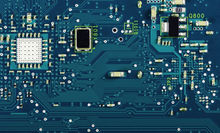
Table of Contents
One of the fundamental aspects of any circuit diagram is the return current path or electrical return path. In a circuit diagram and a schematic diagram, the path the current follows to return to the low potential side of a power source should be obvious, but it may not be so obvious in a PCB. To quote the great Eric Bogatin at his PCB West 2019 presentation, the distinction between a schematic diagram and a PCB layout lives in the white space of your schematic. In other words, you need to consider the geometry of your PCB layout in order to understand at a deep level how current moves throughout the system.
The geometry of your traces and internal planes is just one aspect that determines the electrical return current path in a PCB layout. The signal itself will, in some ways, choose its own return path. Once a designer understands how the geometry and the characteristics of a signal affect the return current path, it becomes easier to determine the return current path for signals without resorting to 2D or 3D field solvers.
What Determines the Electrical Return Path in a PCB?
We like to say that currently follows the path of least resistance, but this is really only true for DC circuits. With time-varying signals, the return current follows the path of least reactance, which is also the path of least impedance. This means the return current path in your PCB is determined entirely by the impedance of the circuit that carries the return current.
If this sounds esoteric, consider for a moment the structure of a modern PCB. Current flows from the power source along supply rails or a power plane, downstream into your components, and finally into the ground plane, where it travels back to the low potential end of the power source. This entire path has some associated impedance.
Going back to electronics 101 for a moment, the impedance seen by the current in your circuits can be split into a resistive portion (independent of frequency) and a reactive portion (dependent on frequency). In reality, any circuit on a real PCB can behave as a purely resistive, purely capacitive, or purely inductive circuit, depending on the geometry, behavior of different components, and frequency of the signal traveling through a circuit. Real linear circuits on a board should be modeled, at minimum, as RLC circuits, even if the circuit does not contain any discrete capacitors or inductors.
Why should a circuit in a PCB layout act like an RLC circuit? This occurs because adjacent conductors are separated by an insulating substrate, which creates some parasitic capacitance. The inductive behavior arises because the current path followed by a current form a closed loop, and the substrate has some magnetic permeability, thus each circuit looks like an and has some parasitic inductance. These parasitics and the natural DC resistance of conductors contribute to the impedance seen by signals as they travel throughout your board. When taken together with the geometry of traces and planes, these collectively determine the path followed by signals as they return to the power supply.
How Signal Frequency Affects the Electrical Return Current Path in a PCB
To get a sense of how the electrical return current path in a PCB is formed, we’ll first look at what happens with DC current in a simple example. The top view in the example layout below shows traces on the surface layer of a PCB leading to an IC. The bottom half of the figure below shows the interior ground plane in the second layer. The two conductors are separated by the insulating substrate, which provides capacitance between the two layers. Note that the capacitor symbols shown below do not indicate the presence of discrete capacitors; think of these as part of a lumped circuit model. (Note: this is actually the reason that every trace in a PCB is really a transmission line; more on this in an upcoming article).
A DC current that originates in the top layer (at the +5 V point) travels directly along the trace, which has the path of least resistance. After the current leaves the IC, it enters the interior layer through a via and travels along the ground plane; it then returns to the supply point on the surface layer through another via. The DC current sees infinite reactance (thus infinite impedance) between the surface layer and the ground plane, meaning the current does not travel directly to the substrate through the lumped capacitance. Once the current enters the ground plane, it follows the path of least resistance back to the GND via. Note that the path of least resistance just happens to be the shortest distance (the straight yellow line) between the two vias.
Return current path in a PCB for DC currents
With any time-varying signal (either a pulse, digital, or analog signal), the situation is different. Because the voltage and current are changing in time, the signal can induce a displacement current through the lumped capacitance in the substrate, which then travels through the ground plane. This means that the return current is produced in the ground plane below the trace. The resistance doesn’t change with frequency, but the reactance provided by the substrate capacitance does depend on frequency. Current tends to be concentrated below the signal trace, which corresponds to the path of least reactance.
Return current path in a PCB for quickly time-varying currents
Note that the yellow lines shown in the top view are slightly offset from the circuit trace for clarity, but hopefully you can see the clear difference between these two situations. The situation obviously becomes more complicated when we have multiple traces, components, and plane layers in a PCB. In reality, the return current will have some approximately Gaussian distribution beneath the trace at high frequencies (~MHz and above). At moderate frequencies (10’s of kHz), there will still be some current that follows the DC return path. Take a look at this article from Bruce Archambeault (Figs. 3-5) to get an idea of what happens at moderate frequencies.
What About Mixed Signal Electrical Return Paths?
With mixed signal boards, controlling your electrical return current paths is even more critical as you should try to prevent digital signals from inducing a current in analog sections of the board. Splitting your layout into analog and digital sections goes a long way toward reducing mixed signal crosstalk. However, you should still make an effort to determine the return current path in your PCB layout to prevent different each type of signal from unintentionally interfering with sensitive components. Francesco Poderico provides an excellent tutorial on determining return paths in mixed signal boards in a recent article.
If you are savvy with your analysis of your layout, then you likely won’t need to run simulations from your design just to determine to return current paths. However, simulation tools and 2D/3D field solvers still provide real value and can be used to verify many of your design choices and the functionality of different circuits in your board.
With the powerful PCB design and analysis tools in Altium Designer, you can analyze all aspects of your schematics and layout, and you can help prevent signal integrity problems that arise in complex PCBs. These tools are built on top of a unified rules-driven design engine, allowing you to perform important DRCs throughout the design process. You’ll also have access to a complete set of manufacturing planning and documentation features in a single platform.
Now you can download a free trial of Altium Designer and learn more about the industry’s best layout, simulation, and production planning tools. Talk to an Altium expert today to learn more.


