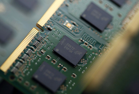
Rigid PCB Vs Flexible PCB: How Adaptable is Your Design Approach

After working on multiple projects for a demanding client, I often relieve my stress by kicking it out at a local martial arts gym. When I was a teenager, I was quite flexible and had no trouble landing kicks. These days, however, my kicks are somewhat restrained by my rigid legs; I’m simply not as flexible as I used to be. Of course, flexibility and rigidity are important concepts outside of the martial arts gym as well. While designing PCBs, for instance, the choice of flex PCB versus rigid PCB can influence your entire design approach.
In electronics, you may find yourself shifting from rigid PCB to flex PCB, as the growth of smart wearables and Internet of Things (IoT) demands electronics in flexible form. Like it or not, flex PCB design skills are slowly becoming a valuable skill in the electronics industry.
When and Why Should You Use Flex PCB?
While the production of flex PCBs may not be the cheapest, its flexibility allows for a higher level of functionality than what rigid PCBs can achieve. Being able to bend without breaking its track enables flex PCB to be fitted easily in smart wearables and devices with very limited space.
Electronics constructed on flex PCBs are also more durable, as the low mass of the PCB significantly decreases any risk of damage from vibrations. Besides that, flex PCBs are made of polyimide, which can tolerate extreme temperatures. This makes flex PCBs ideal for devices that operate in high-heat environments. Due to their various benefits, flex PCBs are growing in demand within the electronics industry.
It’s bend or break when it comes to flex PCB design.
Considerations When Designing With Flex PCB
When you’re working with a rigid PCB, your worries probably involve squeezing hundreds of components into a tiny PCB or ensuring that analog parts are properly separated from digital ones. In rigid PCB design, your concerns are purely electronics-based. When you shift to flex PCB design, these concerns shift as well.
Originally used in the World War II era, flex PCBs were initially designed to replace hand-built wire harnesses that were prone to human error. The tiny strips of copper in flex PCBs allow for high-density connections. However, electronics skills alone are not enough to build flex PCBs; mechanical knowledge is needed, as copper tracks and components are subjected to mechanical stress due to the nature of the flex PCB.
An important criterion when designing with flex PCB is the bend ratio. Expressed as a ratio of bend radius against the flex PCB thickness, the bend ratio cannot dip below a minimum threshold. If the bend ratio dips, the circuit becomes vulnerable to mechanical failure. Additionally, the bend area of the flex PCB is particularly sensitive to changes in copper width or direction. Holes in the bend area should also be avoided at all cost.
Along with these considerations, here are additional flex PCB design tips to help you minimize production defects:
Avoid I-Beam Stacking: In rigid PCB design, you can have traces running parallel on top of each other at the top and bottom layers without any issues. But when you’re designing flex PCBs, traces should not be stacked on top of each other as this could decrease circuit flexibility.
Routing Corners in Bend Area: When you’re routing corners in a rigid PCB, your concern is whether right-angled corners cause electromagnetic interference (EMI) or generate heat points in a high current circuit. The shape of the tracks in the bend area can easily make or break your flex PCB. Avoiding changing the track direction in the bend area is always recommended. If change is inevitable, a soft corner is preferred instead of the typical 45° sharp corner common in rigid PCBs.
Compression Versus Stretching: In rigid PCBs, there are typically no hard rules about routing small conductors less than 7 mils. However, in flex PCB design, the effects of compression and stretching need to be considered. Routing small conductors on the inner side of the bend can reduce the likelihood of track damage, as smaller conductors better tolerate being compressed than being stressed.
Make Conductor Width Bigger When Possible: Flex PCB saves precious space in your electronics. But if you think having tiny tracks is a good approach, you couldn’t be further from the truth. The rule of thumb with track width is that it should be at least five times the thickness of the copper foil of the flex PCB. You should make this rule applicable for all your tracks, except in certain situations where they need to squeeze through the small spaces between pads.
Arm yourself with the right wiring and routing that’ll do the job for your designs.
Working on flex PCBs can be easier with PCB design software made to enhance your flexibility without additional restrictions. Altium Designer’s board planning mode enables you to easily specify the bending line and radius when you organize stack up layers. If you want to work in your board layout efficiently, let your design software do the hard work for you in visualizing the design.
Need more assistance with your flex PCB design? Contact an expert at Altium.
Related Resources


Related Technical Documentation


Take advantage of the world's
most trusted PCB design system.
One interface. One data
model. Endless possibilities.
Effortlessly collaborate with
mechanical designers.
The world's most trusted
PCB design platform
Best in class interactive
routing
View License Options
Thank you, you are now subscribed to updates.