Hybrid or Compact: Fractal Antennas in PCB Design
The Mandelbrot Set was always a popular poster among my fellow students when I was in college. The zoomed-out picture hung on dorm room walls and even appeared on some graphic t-shirts. The fact that no one seemed to know about the Mandelbrot Set or understand fractals didn’t seem to matter. It wasn’t until much later that I realized how useful fractals could be in designing antennas. There are many antennas in the PCB world including: microstrip patch antenna, wideband antenna, wifi antenna, helical antenna, loop antenna, bowtie antenna, and many more!
More than just a mathematical peculiarity and source of interesting pictures on the internet, fractal geometries can be used to design antennas for wireless communication. These antennas tend to have a small form factor and can be designed to operate as multiband or broadband antennas. Like other antennas used in wireless electronic devices, these antennas can be fabricated on PCBs and imbue wireless devices with considerable versatility.
Fractal Antennas
Just as its name suggests, a fractal antenna uses a fractal geometry. If you are not familiar with famous images like the Mandelbrot Set, a fractal geometry contains repeating geometric patterns. Your fractal antenna geometry does not need to be anywhere near as complex as the Mandelbrot set; relatively simple fractals can be used as antennas in PCBs.
Different portions of the structure have different resonant frequencies, and the mathematical relationship between frequencies is determined by the fractal PCB antenna design. It’s also possible to change the reactance of an antenna by changing the shape of its conductors while keeping the overall size of the PCB antenna constant.
Although the electrical length of a fractal antenna is long, the entire fractal has a smaller footprint than a stripline antenna with the same frequency. This smaller footprint, bandwidth tunability, and the ability to build multiband capabilities make fractal antennas desirable in many applications.
One example is in Bluetooth devices, where communication between devices occurs over 80 channels within the 2.45 GHz band. Rather than use multiple antennas, most PCBs used in mobile phones use a single Sierpinski Carpet fractal antenna to save board space.
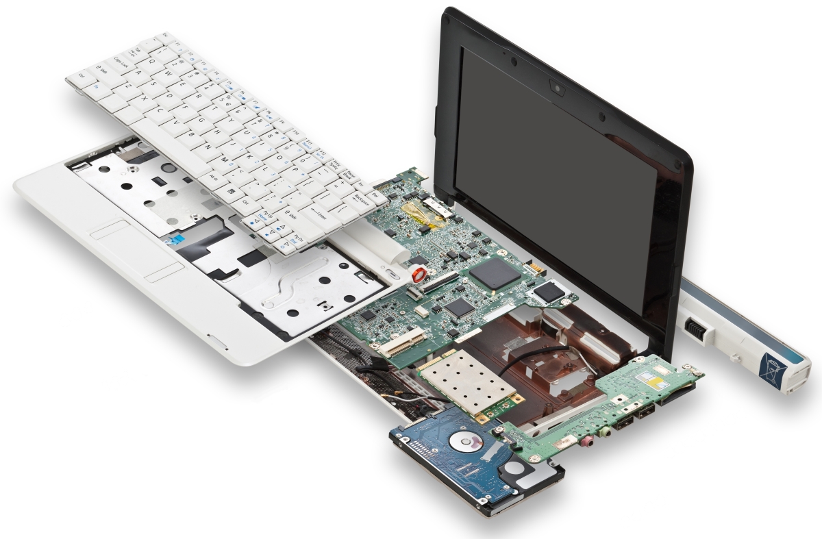
Layout of PCB devices, especially for antennas, is particularly important
Layout Considerations
Designing and laying out a fractal antenna is a major space saver due to its ability to simultaneously function as multiple antennas. Rather than build multiple antennas or use multiple chips for reception in different RF bands, the frequencies in a multiband antenna can be set to coincide with RF communication bands.
Fractals with high iteration number will have reception at a number of higher frequency bands that may not be usable. However, response at the extra bands can be removed through filtering. Sensitivity at the remaining desired bands can be improved using an LNA. Multiband LNAs are still in the research stage, but dual-band LNAs and broadband LNAs that can span multiple frequency bands are commercially available.
Whether you’re designing a single band, dual-band, or a multiband fractal antenna, these antennas should not be placed above the ground plane and are typically placed at the edge of the board. These antennas are commonly implemented as monopole antennas, allowing near omnidirectional emission. Fractal antennas can also be designed as a dipole antenna.
Ground plane placement and geometry can affect the emission pattern and bandwidth. Many fractal antenna layouts will extend the ground plane up to the edge of the antenna, similar to the case of conventional antennas.
Making minor modifications to the ground plane, like cutting notches or geometric shapes into the ground conductor, has been shown to greatly affect the bandwidth at the desired frequency bands, as well as the impedance bandwidth. In addition to increasing the frequency bandwidth, this also has the benefit of bringing the total impedance closer to 50 Ohms.
Impedance Matching and Simulation
Just like any components operating with radio frequencies, fractal antennas must be impedance matched to other components on the PCB. But unlike typical multiband antennas, fractal antennas tend to have ultrawide impedance bandwidths. This means that multiple bands can be impedance matched relatively easily and do not require the iterative process required for a typical dual-band antenna.
Example of a Smith Chart for impedance matching of antennas
The fractal structure can be thought of as an equivalent combination of inductors and capacitors. But modeling the equivalent impedance of the antenna is not always as simple as reducing to a pair of these circuit elements. You can analyze the behavior of your antenna and determine if any impedance matching is required with a Smith Chart.
Fractal antennas are still a major subject of research and development in the microwave community, and only the more popular antennas have well-understood design rules. Analyzing your fractal antenna design requires simulation software.
Altium Designer® has advanced functionality and an extensive component that enables you to add multiband or broadband fractal antennas into your PCB design. It also has excellent CAD tools that allow you to design your own fractal antenna.
Talk to an Altium expert today to learn more.


