Cross-Probing Electronic Components in PCB BOM Software with a 1968 Bel Air
Table of Contents
I have a friend who once bought a 1968 Bel Air that was in immaculate condition inside and out. There was one problem though: the engine ran really rough. Since my friend was pretty good at working on cars, he bought it for a very low price thinking that he could simply tune it up. It didn’t work though, and my friend came to realize why this beautiful car had come with such a cheap price tag. Then he took a closer look under the hood and was amazed to find that the spark plug wires had been routed for the shortest distance instead of being correctly routed to their assigned plugs. With the spark plugs miss-wired like this, it was amazing that the engine ran at all. Once he corrected the problem he had a car that not only looked great but ran great as well.
Not only do I wish that I had been lucky enough to find and buy that car myself, but that story also reminds me of the importance of being able to see what we are connected to. My friend had to really search before he noticed that the plug wires were connected to the wrong plugs. In printed circuit board design, we don’t always see how our components and nets are connected to the schematic either. Fortunately, our layout tools can help us with this by cross-probing between the schematic and the layout.
Cross-probing or cross-referencing will automatically select an object in the schematic when you select the corresponding object on the layout side, and vice versa. You can select in the schematic to help organize your layout, and when looking for a component on the schematic you can simply select it in the layout. Slip behind the steering wheel and let your cross-probing from your layout and schematic into the bill of materials turn into a cruise.
Cross-Probing Advantages in Layout
Just like my friend and I could give you all the details which make that Bel Air shine, I can also give you the traits which makes cross-probing so convenient. When you are laying out your PCB, the ability to cross-reference will give you real benefits:
-
Component organization: If you want to organize your layout without using the cross-probing, you will need to find the components on the schematic, note their reference designators, and then search for those same in the layout. This is a very cumbersome process. Cross-probing gives you the ability to select the components you want in the schematic, and have the corresponding in layout automatically select. This allows you to easily organize a pile of unplaced components in the layout.
-
Placing according to the schematic flow: This is really an extension of the first point, but it is an important one. After you organize your components you can then create circuitry patterns on the layout according to the logic flow in the schematic. Being able to cross-reference allows you to do this by selecting the components in the schematic to work with on the layout side.
-
Net selection: In the same way that you can select components in the layout by cross-probing from the schematic, you can also select nets. This allows you to quickly find critical nets such as clocks or differential pairs. If you need to add multiple nets to net classes on the layout side, you can do this easily by selecting those nets in the schematic so that they are then automatically selected on the layout side.
Cross-Probing Advantages in the Schematic
Cross-probing between the schematic and the layout works both ways, so anything that you select on the layout will automatically select in the schematic. This gives you the ability to trace back a circuit from the layout to see how it is represented in the schematic. Test technicians will also benefit from cross-probing by having the layout tools open as they debug the board. By finding and selecting the part in the layout that they are currently testing, the schematic will automatically select the corresponding component for them.
I have found that cross-probing also really benefits a design review. With the schematic and the layout presented side-by-side, participants in the review can check from either direction. Once an area that they have concerns about is selected, the cross-probing will then select and show them the corresponding circuitry on the other side.
Cross-Probing into the Bill of Materials
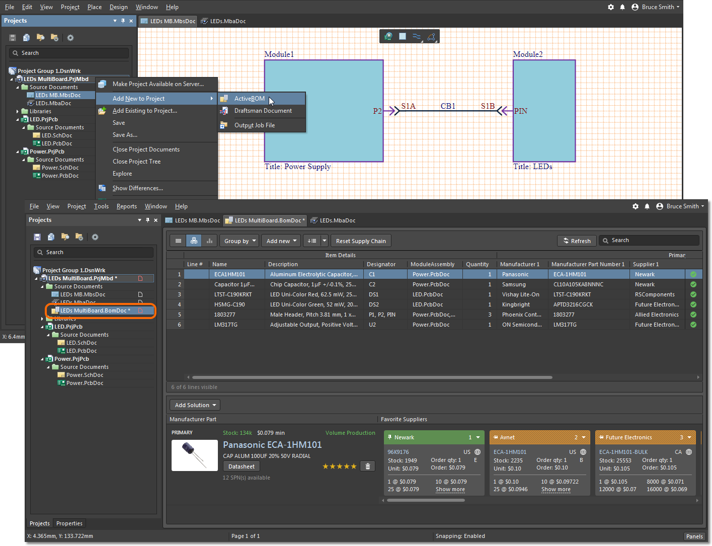
With the ability to cross-probe and cross-reference from the schematic or layout into the and back again, a whole new world of functionality has been opened up to the PCB design team. Designers are able to find a specific part by looking at a sorted first without having to search through the schematic or the layout first. This is extremely helpful in looking for where specific are being used in a design, especially when those need to be updated or changed.
Design reviews also benefit greatly from cross-probing. When one schematic part is questioned, design teams can immediately cross-probe over to the to find out how many of those are being used in the design. This will give the team immediate access to the reference designators of those, and the ability to select and display them as well.
Cross-probing is a great way to keep your wires straight and to know what you are connected to. Additionally, the ability to cross-reference into the now provides you with yet another powerful tool that will help you with your PCB design.
PCB design software, like Altium, has the cross-probing functionality between the schematic, layout and the that we have been talking about here. Active connects the bill of materials with the rest of your design through the unified design platform giving you control over your design that you need. Find out more information on how Altium’s Active can help cross-reference your next PCB design by talking to an expert at Altium.


