Electric Distribution Systems and PCBs: Power Distribution Network Design
Table of Contents

For those of you who have only experienced the brilliant high power of LED, Xenon, or Halogen headlights in today’s modern cars, you may not realize how fortunate you are. My first car was old enough that its headlights could have been candles. One year I received Halogen fog lights for my birthday, and the difference at night was amazing. Not only could I now see what was next to the car in the dark but the fog lights almost out-distanced the regular headlights as well.
Being able to see where you are going is important in many areas of our lives. Whether it’s going downstairs into a dark basement, driving at night, or even laying out a printed circuit board we’ve got to have the lights on. That may sound odd considering that there is usually plenty of light in our places of work and our computer monitors typically provide more than enough illumination to get the job done.
Previously, designing the power distribution network () has been left in the dark. Designing a is much more important than its history of making sure you have a good size power and ground plane. Now as PCBs have grown in technology while shrinking in size, having a well-designed has become one of the chief cornerstones of the design. A PDN Analyzer™can guide you through the guesswork of designing your power distribution network.
The Importance of your Power Distribution Network Design
The goal of your PCB’s is to provide clean power and reference voltage to the active devices. An inadequate can contribute to signal integrity issues. Also, electromagnetic compliancy (EMC) problems can be due to excessive noise on the PDN as it connects to external cables and radiates emissions.
It is typical for high speed designs to contain multiple power supplies, and the PDN must be designed to handle all of the different current requirements. The goal is to design a stable PDN for all the required power supplies with as low of an effective impedance as possible. This should be planned for before component placement even begins so that you know ahead of time how it should all be laid out.
The Problems Designers Face
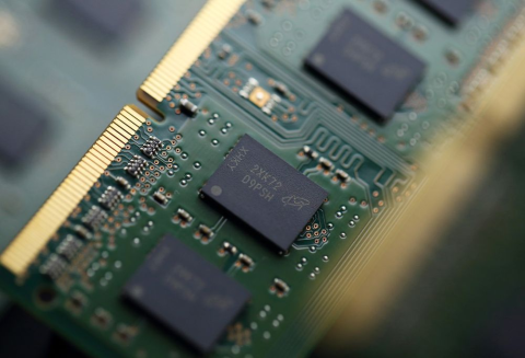
The problem that designers face is that the planes or traces used for delivering power and ground are rarely that simple to work with. In addition to the power needs, a designer needs to make sure that the planes are adequate for signal return paths. Thru-hole devices, vias, and even slots for mechanical purposes can also punch holes in what would have been a good design.
Another hazard to a well-designed is split planes. When a splits a plane for digital and power ground, they need to make sure that they have the appropriate devices and signals over the digital ground. Having to split planes like this can add another level of complexity to the . Additionally, buried traces will cut planes into multiple which is yet another headache for the design of the .
How a PDN Analyzer Can Help
With all of the challenges to designing a good PDN, a PDN Analyzer tool is essential for providing a visual display of the power distribution network. PCB designers can see in real-time what potential problems are in their PDNs in order to correct them.
A PDN Analyzer will allow you to define your power nets as sources, loads and grounds. It will also allow you to define your source and load devices. Once set up you will get a visual display of the following problems:
- Excessive copper.
- Isolated areas of copper.
- Insufficient copper.
- Uncontrolled voltage drops.
- Marginal voltages at device power pins.
A PDN Analyzer can turn up the lights in what used to be the darkness of power distribution network design and show you the way to correctly design the on your printed circuit board. This will save you from having to create multiple board spins in order to identify and correct problems.
To expertly move from schematic capture, through PCB layout, and to creating manufacturing output files consider PCB design software such as Altium Designer® . Thankfully, it also contains a PDN Analyzer tool with all the functionality that we’ve been talking about here. With it, you can find and resolve issues during layout before the board is manufactured.
Would you like to find out more about how Altium can help you with your power delivery network layout on your next PCB design? Talk to an expert at Altium.
Check out Altium in action...
Powerful PCB Design
Related Resources


Related Technical Documentation


Take advantage of the world's
most trusted PCB design system.
One interface. One data
model. Endless possibilities.
Effortlessly collaborate with
mechanical designers.
The world's most trusted
PCB design platform
Best in class interactive
routing
View License Options
Thank you, you are now subscribed to updates.