Design for Test: Determining the Value of the JTAG Interface During the Schematic Stage
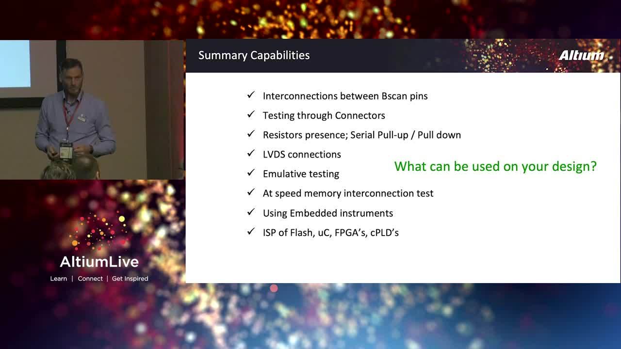
After a brief explanation about modern test methodologies and in-system programming capabilities via the JTAG interface on chip, board, and system level, the focus of this presentation will be on the necessity and ways for improving your design for testing (DFT) and fast in-system programming. This is best done during the schematic stage. Studies and experience show that if you do, your company will substantially save engineering time and build more reliable products.
View the presentation slides:
Sign up to pre-register for AltiumLive next year or try Altium Designer today.
About Author
Related Resources

Table of Contents
<ul><li class="b-hide__item"><a href="#view-the-presentation-slides">View the presentation slides: </a></li></ul>
Take advantage of the world's
most trusted PCB design system.
One interface. One data
model. Endless possibilities.
Effortlessly collaborate with
mechanical designers.
The world's most trusted
PCB design platform
Best in class interactive
routing
View License Options
Thank you, you are now subscribed to updates.