Skip to main content
Mobile menu
PCB Design
Altium Designer
World’s Most Popular PCB Design Software
CircuitStudio
Entry Level, Professional PCB Design Tool
CircuitMaker
Free PCB design for makers, open source and non-profits
Why Switch to Altium
See why and how to switch to Altium from other PCB design tools
Solutions
For Enterprise
The Last Mile of Digital Transformation
For Parts and Data
Extensive, Easy-to-Use Search Engine for Electronic Parts
Altium 365
Resources & Support
Explore Products
Free Trials
Downloads
Extensions
Free Altium 365 Tools
Online PCB Viewer
Resources & Support
Altium / Renesas Scheme: Information for Shareholders
Renesas/Altium CEO Letter To Customers
All Resources
Support Center
Documentation
Altium Community
Forum
Bug Crunch
Ideas
Education Programs
Professional Training / Certification
University / College Educators
University / College Students
Webinars
Store
Search Open
Search
Search Close
Sign In
PCB Design Engineers
Main menu
Home
PCB Design
Collaboration
Component Creation
Data Management
Design Outputs
ECAD/MCAD
HDI Design
High Speed Design
Multi-Board
PCB Layout
PCB Routing
PCB Supply Chain
Power Integrity
RF Design
Rigid Flex
Schematic Capture
Signal Integrity
Simulation
Software
Altium 365
Altium Designer
Enterprise Solutions
PDN Analyzer
Upverter
Education
Programs
Altium Academy
Engineering News
Guide Books
Newsletters
Podcasts
Projects
Training Courses
Webinars
Whitepapers
FREE TRIALS
PCB Design Engineers
Build High Density Interconnect PCBs with Skip Vias
All high-density PCBs rely on specific via styles to make connections into the inner layers without taking up space for routing. This is always driven by the components used in the PCB, namely fine-pitch BGAs with many high pin counts. One of the options for routing into inner layers as part of fanout routing is to use skip vias. Type-I HDI stackups will include skip vias as part of their routing options in an attempt to avoid the use of buried
Read Article
Creating Multiple-Part Symbols for a PCB in Altium Designer
How to create multi-part components and symbols in Altium Designer
®
. Build a symbol manually or use an advanced symbol generator to do the heavy lifting of symbol creation for you.
Read Article
How to Create Schematic Symbols in Altium Designer
A step by step walk through of the Schematic Symbol Generation Tool in Altium Designer.
Read Article
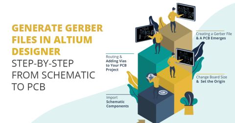
How to Make PCB Gerber Files in Altium Designer Step-by-Step
Looking for the best approach for CAM jobs? Learn how to make PCB Gerber files in Altium Designer from your circuit board layout. Altium's CAM tools can help you quickly create PCB Gerber files.
Read Article
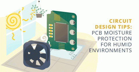
Circuit Design Tips: PCB Moisture Protection for Humid Environments
Learn more about implementing PCB moisture protection and storage in your design to prevent corrosion and board failure.
Read Article
Are Fiducial Marker Placements on PCBs Still Necessary with Modern Manufacturing Capabilities?
In PCB design, a fiducial marker is a rounded shape of copper that acts as a reference point for pick and place assembly machines. Fiducial PCB markers help machines recognize the orientation of the PCB as it passes through SMT. Based on the PCB orientation and the prior orientation of components on reels, the machine can be programmed to rotate components by specific amounts to ensure accurate placement on their land patterns. Placement of
Read Article
How to Choose the Best Desktop Reflow Oven for PCB Assembly
Desktop reflow ovens come with a big price tag range. So which capabilities should you target? Learn more about desktop reflow ovens in this article.
Read Article
Getting Started with Design Miniaturization: Impacts and Complexity
Since they’ve been created, electronics have been getting smaller, faster, and more efficient. But when you try to cram more components, pins, and connections in a smaller sized board, you’re going to have some problems. These challenges include heat, BGA breakouts and size itself, meaning how are you going to fit your board in that small, oddly shaped enclosure. Here are a few quick stats: Board area has remained relatively constant, while the
Read Article
Challenges with Rigid-Flex Design
To learn more about this topic please see the full solution - Challenges with Rigid-Flex Design - at Altium.com.
Read Article
PCB Design Tools
Utilizing the available PCB design tools to their maximum potential allows designers to strike the perfect balance of passion and productivity in their work. Data from top performing designers demonstrates how these tools can lead to more successful outcomes in both business and engineering when used correctly. Key findings include: Best-in-Class companies are more likely to improve designer productivity through tool and process efficiency. The
Read Article
Solving Modern PCB Layout Challenges
PCB technology advances are a two-edged sword. They have increased the power and applicability of electronics. But they also make PCB layout more difficult, raising the risk of longer time-to-market cycles and higher product costs. Designers can mitigate these risks by using a unified PCB layout software package that provides the automation necessary to bring products to market quickly and on-budget. INTRODUCTION “Honey, I shrunk the kids.” “It’s
Read Article
59:39
Altium Aberdeen
Watch Video
How to Avoid Common PCB Signal Integrity Issues in Your Designs
Learn the common PCB signal integrity approaches to help eliminate basic system level failures.
Read Article
The Hateful Five of PCB Manufacturing
You just completed your last design review, got that needed approval signature, and the finish line has never been closer, or so you think. Even after your components are sourced and your board is laid out perfectly, the biggest challenge is yet to come - ensuring that all those months of design and team effort don’t go to waste when it comes time to communicate design intent to manufacturing. But how do you navigate this stage of your post
Read Article
The Power of Integration - Why Analysis Belongs to PCB Designers
PCB designers often rely on simulation tools or prototypes for their network data, but this approach can disrupt design flow and drain funds. What if designers were capable of analyzing their network during the board layout process? Read on to find out how designers are increasing productivity with access to analysis data at design time. As the complexity of our product designs increases each year, so do the requirements of our designs. And
Read Article
The Power of PDN Analysis Automation
Relying on a prototype for analysis into your network costs time and money. Leveraging automation tools like the PDN Analyzer
™
can reduce costs and allow the engineer to optimize designs without relying on a prototype. Read on for more information. “There’s nothing worse than an engineer dropping a via stitch array late in the RF design process and leaving barely any power plane copper left to carry current on a board makes it painfully obvious
Read Article
PCB Design Variant Management to Synchronize Designs
Product customization is increasingly popular to satisfy customer demand as both time-to-market and the complexity of products continue upward without abatement. By making variations of a baseline product, the new products can address different markets and requirements. But how do you go about keeping synchronized PCB variants? Making the Case for PCB Design Variants You are developing a PCB layout for a smartwatch that comes in three different
Read Article
Pagination
First page
« First
Previous page
‹‹
Page
3
Page
4
Page
5
Page
6
Page
7
Current page
8