Add USB Type-C Power Delivery to Your Designs!
Introduction
USB Type-C Power Delivery (PD) is becoming increasingly prevalent in hardware designs, offering hardware the ability to source or sink up to 100W (and even up to 240W in the updated 2.1 specification!) of power. In this article, we will explore the fundamentals of USB Type-C Power Delivery and learn how to easily incorporate a dedicated PD IC into your own designs.

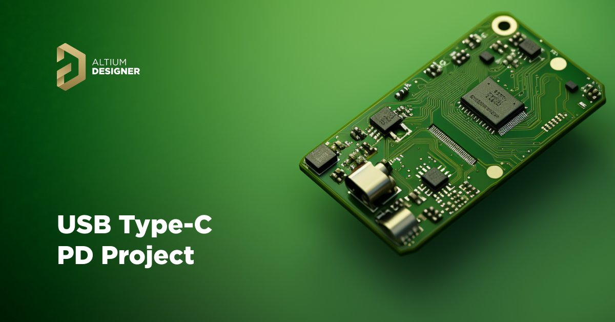
Figure 1 USB Type-C PD Demo Board
USB connectors and their respective cables, such as USB Type-A and Type-B have been the standard for data and power connections for most of USB’s history. However, these interfaces have limitations in terms of power delivery. In contrast, USB Type-C offers a more versatile solution with higher current-handling-capable pins and communication channel pins for power negotiation.

Figure 2 USB Type-C Connector (Source: Farnell)

Figure 3 USB-C Connector Pin-Out (Source: All About Circuits)
The pins we are interested in, in particular for power delivery, are of course the power and ground pins (VBUS, GND) but also the communication channel pins (CC1, CC2). These CC pins can be used to negotiate power between devices (sinks and sources).
We will not go into detail regarding the USB Type-C PD specification here, but I would strongly recommend that you check out two primers by Texas Instruments and USB-IF.
Additionally, make sure to check out the full video walkthrough of a USB Type-C PD-based hardware design here.
USB Type-C PD Controller IC
A very simple method of utilising USB Type-C delivery, should you only require up to 15W of power, is in fact without ‘direct negotiation’. This is achieved by pulling down the CC1 and CC1 lines via separate 5.1kOhm resistors on your device that will sink current. Keep in mind however that this method does not allow for checking if the source can support this power.

Figure 4 CC 5.1k Pull-Down Resistors
A better approach to incorporating USB Type-C Power Delivery into your designs, is by using a USB Type-C PD controller IC. These integrated circuits are designed to handle the negotiation and power delivery process. Various manufacturers produce these ICs, offering different packages and capabilities to suit your specific requirements. Make sure to use Octopart to check out the many different USB PD IC options!

Figure 5 Infineon USB-C PD IC (Source: Infineon)
We will focus on the Infineon CYPD3177, a USB Type-C PD controller capable of supporting USB PD 3.0 Revision 2.0, offering up to 100 watts of power delivery (sink only). This IC makes it very easy to negotiate different voltage and current requirements within the USB PD protocol and does not require much configuration and external circuitry.
Additionally, the CYPD3177 features an integrated I²C block, which allows you to control the device using an external host controller. This opens up opportunities to customise and fine-tune the USB PD settings beyond basic voltage and current settings.
Schematic
Luckily for us, Infineon provides a very good datasheet, as well as a hardware design reference for their evaluation board. All information we need to create the schematic is contained in those documents.
A simplified reference schematic is shown below:

Figure 6 Reference Schematic (Source: Infineon)
Power In and USB Type-C Connector
Connections to the USB Type-C connector are VBUS, and GND, as well as the CC1/CC2 pins. Be sure to add in ESD protection (and filtering, if necessary) – depending on your application’s requirements.
The IC is powered via the VBUS_IN pin (pin 18) and internally generates its own required voltages, including a low-current +3.3V supply which we can use for some of the external circuitry. This is very handy, as the IC does not need an additional, external supply.
As usual, we require some decoupling capacitors at the VCCD (pin 24) and VDDD (pin 23) as shown in the reference schematic.
Power Out and FETs
You will have noticed the two sets of PFET transistors at the top of the schematic. The top-most set is controlled by the PD IC (VBUS_FET_EN, pin 3) to act as a load switch. Once negotiation is complete via the CC lines, the switch is closed to allow power to flow from the source attached to the USB Type-C connector through to the relevant sub-system of your device.
The PFET set below has a similar switch function. However, this switch is only closed by the PD IC (SAFE_PWR_EN, pin 4) should the negotiation fail, and the system falls back to the typical +5V (and lower current) on the VBUS line.
Suitable transistors (for example, low loss, sufficient current-handling capabilities, as well as suitable gate-source and drain-source voltage limits), as well as external circuitry (resistors, capacitors, and diodes) need to be chosen according to the datasheet recommendations. You can also follow the previously-linked reference design for specific part choices.
Setting Voltage and Current Requirements
The PD IC can be controlled either via the aforementioned I²C interface (HPI_SDA and HPI_SCL, pins 12 and 13), or very simply via external strapping resistors (ISNK_COARSE, ISNK_FINE, VBUS_MIN, and VBUS_MAX, pins 5, 6, 1, and 2).
For the strapping resistor option, the voltage at the relevant pins is sampled at IC start-up and that determines the range of negotiated voltage, as well as the maximum current required. This is shown in the table below:

Figure 7 Strapping Resistor Options
Miscellaneous
The previous circuitry is the minimum amount we need for this PD IC to function – as you can see, there is not much to it! However, there are some additional features that may be useful, depending on your specific application.
For example, the I²C pins can be connected to a host controller for further configuration, the FLIP pin (pin 10) can be used to indicate the orientation of the attached USB Type-C cable and to set if the device is data capable or not, and the FAULT pin (pin 9) indicates if the source cannot supply the required voltage or current or if an over-voltage event was detected.
PCB
The PCB design for this particular PD IC is straightforward, despite the IC being in a QFN-style package. The image below shows the hardware incorporated on a simple, two-layer board in Altium Designer, as there are not any high-frequency components to this design (the ‘fastest’ being the rise/fall-times of the I²C interface).
The top layer is used for power and signal routing, whereas the bottom layer is dedicated to a solid, mostly uninterrupted ground plane. The fallback supply option is not used here.

Figure 8 USB-C PD IC PCB (3D)
What we need to take care of is that our power interconnects are sufficiently sized to reduce DC IR drop and to keep the temperature rises to a sensible level. I would suggest keeping your power-carrying traces (or polygons even) as short as reasonably possible and to calculate the required trace widths using an IPC-2221 calculator. Power-handling components, such as the PFET switches are thus also placed close to the relevant other power components.
If there are large copper imbalances on sides of the same component, aim to use thermal relieves to make the assembly process easier.
Additionally, the decoupling and bypass capacitors should be placed close to the relevant pins of the PD IC. We can place ‘less-critical’ parts, such as the strapping resistors further away from the QFN package IC, as this leaves us ample space for fanning out the device.

Figure 9 USB Type-C PD PCB Routing
Conclusion
This article outlined the basics of implementing USB Type-C power delivery in your own hardware designs. As we saw, the process – thanks to dedicated PD ICs – is very straightforward, with not many additional parts required.
Make sure to check out the full design walkthrough video here, which covers some of the finer details and follow along with a free trial of Altium Designer!


