How Embedded Design Teams Can Simplify I/O and Routing
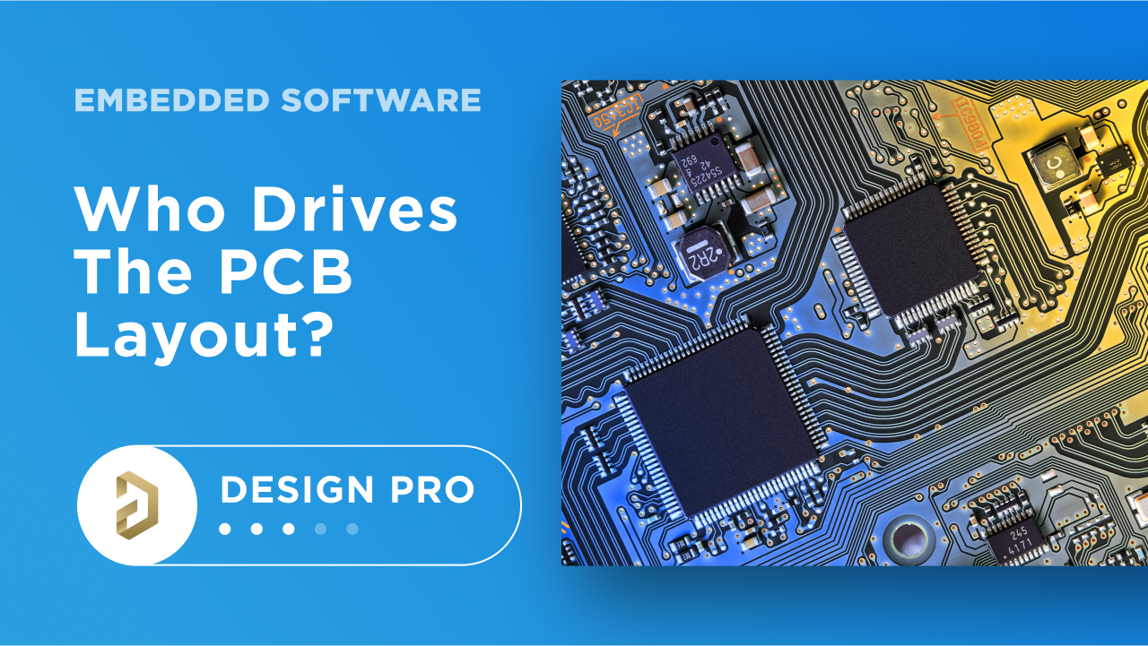
Real electronic products have been slowly getting smarter, both from the implementation of an embedded application and connections back to a cloud platform or application. Embedded development teams have to work together to create these new generations of products. One area where the PCB layout engineer, embedded developer, and even the MCAD engineer can get delayed in finishing a project is in I/O selection. This happens whenever you have connectors, peripherals, and a host processor.
So, to help keep things simple for both sides, I want to share some of my experience working with embedded developers to optimize I/O selection and the overall process for completing the PCB layout. With a bit of collaboration on the front end, you can make PCB routing and embedded development easier on the backend.
Who Does What in Embedded Development?
I take the view that each member of the development team should understand what the other team members need to be successful. This is also about efficient use of resources, avoiding engineering quagmires that take days to resolve, and getting to market quickly.
|
|
|
|
|
|
|
|
|
|
|
|
|
|
|
|
I put an asterisk (*) on the pin list entries because the exact process for assigning I/Os depends on the specific component being used to run the embedded application. Is it a simple MCU, where the available I/Os are fixed in specific locations, or is it an FPGA that can have a customized pinout in certain banks? The other aspect is connectors: is the pinout standardized, is the pinout set by another board in the assembly, or can it be customized?
This is where we can start to see the challenge involved in a PCB designer and embedded developer working together on I/O selection. How can the two sides come together and nail down pinouts, I/O selection, and ultimately the PCB layout?
Embedded Developer Defines PCB Requirements
In my opinion, this works best when the pinout on the main processor is flexible, i.e., the application will be instantiated in an FPGA. In this case, the I/Os can be set by the developer in the device logic, and the result is that the PCB designer will have to work with the pin assignments they are given.
The problem is this: if pin assignments are given on an individual pin basis, you may not get optimal routing, resulting in a mess of connections crossing over each other to get to components. Instead, if the embedded developer just gives bank assignments to the PCB designer, then the PCB designer can choose pins within a bank to make optimal connections.

By assigning banks on an FPGA instead of a specific pinout, the designer can use a tool like a pin swapping to move I/O assignments within a pin bank. If pin swapping is desirable, then a custom schematic symbol might be required in order to properly separate pins into their respective banks. Using a custom symbol enables a much faster grouping of pins for pin-swapping operations while routing the PCB.
PCB Designer Defines Embedded Requirements
In my opinion, this works best when the pinout on the main processor is fixed, i.e., an MCU and its peripherals. In an MCU, the I/O locations are basically fixed. You can have some flexibility in terms of how each I/O is used, for example when using a bank of GPIOs. However, pin or function assignments for standard interfaces may be fixed (e.g., SPI, ADC pins, PWM pins, I2C, etc.).
In this case, I think it’s best if the PCB designer selects the pins they will use to match with different components. The PCB designer has to choose within a fixed pinout, so they will have to work out how to place components in such a way that the PCB layout is solvable. Once placed and routed, it’s the PCB designer’s job to tell the embedded developer which pins are being used for certain functions.

What if a Connector Pinout is Standardized?
When the pinout on your connector is standardized, then it’s a bit of a wildcard. I say this because “standardized” can mean two different things:
- The pinout could be part of a standard interface (Ethernet, USB, etc.)
- The pinout could be set by another board in the assembly or system
If neither of these is the case, then your pinout is customizable. In projects where I’ve dealt with other boards in a larger assembly, we often have the freedom to set a pinout, usually because we were building both boards. In any case, the two sides have to work together to figure out an objectively “best” pinout for the connector and how this matches up with the processor.
Teams that need to collaborate on complex products can access a complete set of collaborative design features when using Altium Designer®. All stakeholders involved in product design can access a complete set of tools for PCB design that can support embedded development tasks, as well as cable and harness design features. When you’ve finished your design, and you want to release files to your manufacturer, the Altium 365™ platform makes it easy to collaborate and share your projects.
We have only scratched the surface of what’s possible with Altium Designer on Altium 365. Start your free trial of Altium Designer + Altium 365 today.


