


Design With Manufacturing: A New View on DFM/DFA


Complete Guide to DFM Analysis
A good friend of mine has a joke about planning a new PCB design for manufacturing: he’ll often ask “have you called your fabricator today?” to stress that you should engage with your manufacturing partner multiple times in the design process. This is something that designers often forget, and it can lead to major headaches ahead of full-scale manufacturing. The fact is, your board should go through multiple rounds of DFM analysis to ensure manufacturability, both in terms of fabrication and assembly.
So when should you start subjecting your design to DFM analysis? Another important question might be: what’s the best way to expedite the DFM analysis process? There is a lot to check in any board, and fully inspecting designs for manufacturability can be time-consuming, especially in complex layouts. Here’s what to expect in DFM analysis and how to get your design through the process quickly.
What Goes Into DFM Analysis for PCBs?
Broadly speaking, DFM analysis applies to anything that needs to be manufactured at scale. Manufactured products need to be designed to fit the process being used for high-volume production, so a design needs to be inspected to ensure nothing in the design will create low yield, defects, or low lifetime. These days, your PCB fabricator and PCB assembler might be on opposite sides of the globe, and it’s critical to ensure they all have access to a single, controlled store of project information to perform DFM analysis.
DFM analysis for PCBs involves checking whether the design will conform to your manufacturer’s processes for fabrication and assembly. Any experienced designer should know that the list of possible design choices that can compromise quality is long. I know that I still haven’t memorized every possible manufacturability problem that might lurk in a design, so I often rely on my fabricator to inspect my boards when I’m about to put in a fabrication run.
Inspect Your Design Often
This brings up an important point: when should you run some DFM checks on your design? If you’re doing some simpler boards, it’s probably fine to rely on your fabricator to run a final DFM check before production; repeated DFM deep-dives just take up excessive time when your fabricator can perform this quickly. For something more advanced, like high-layer count mixedsignal boards with tight clearances and multiple signaling standards, multiple DFM analysis runs are necessary to catch potential quality problems early.
The best way to prevent unnecessary design changes before manufacturing is to do DFM analysis at several different times:
- When selecting components: This mostly relates to passive component sizes, particularly 0201 and 01005. If you must use these small components, just make sure your manufacturer can handle these.
- During floorplanning: At this point, we’re still determining some basic aspects of the board like possible layer count, range of trace widths, via sizes, whether we’ll need to go to HDI, which PCB laminates to use, and which IPC Producibility Level will be applicable to the design.
- After component placement: Once you’ve placed components, consider the assembly process, particularly regarding soldering in double-sided SMD boards. Also think about how any grounded components will solder to their reference plane and whether they need thermal reliefs.
- While planning the stackup: You’d be surprised how many stackups need to be modified before a design can be put into fab. This one is as simple as asking your fabricator for a verified stackup table.
- After generating Gerbers: Some defects are easier to see in your Gerber files, so it’s best to scan your Gerbers for things like overlapping drill hits and via aspect ratios.
- In collaboration with the MCAD team: In some cases, placement of solderable connectors or other mechanical elements can create excessively tight clearances.
There are a few of these points that are worth elaborating on as they may not be often discussed in some other articles.
Component Clearances
Some points that apply to connectors will apply to any other component, but there is one other point around clearances that is worth checking. Make sure you have allowed for expansion during assembly, especially on connectors with a plastic shroud or base. If two components are too close and they expand during soldering, they can both lift off the board during assembly.

Checking clearances in DFM analysis would have helped us anticipate component liftoff during a recent fab run.
Looking at Footprints
Obviously, you should put in the effort to make sure your footprints are verified. This can be done manually, or by only using verified components direct from manufacturers when they are available. However, once a footprint goes into the layout, you’ll need to check solder mask openings, clearance to vias, clearance to other components, via aspect ratios, and more. If you’re not using software with the right rules-checking features, you might leave a thermal pad f loating, or you might place a drill hit too close to a solder fillet. You can look at the PCB layout directly, but it’s perfectly fine to generate preliminary Gerbers and compare your layers (see below).

You can spot components that need solder mask openings and teardrops from interim Gerber files.
Stackup Check
It might sound simplistic, but you’ll pass this one with flying colors if you just ask your fabricator for a stackup with your desired layer count and layer arrangement. They’ve already done the DFM analysis needed to ensure specific layer stacks will pass through their process. They’ll give you the trace width, trace spacing (for differential pairs), and layer thickness you’ll need to use with your desired laminate materials. In some cases, you might be surprised to find that your desired laminate material is unavailable and you’ll need to use a close equivalent.

If you contact your fabricator early, they’ll send you a qualified stackup table.
For 4-layer stackups, you’ll likely receive the standard 8mil/40mil/8mil S/P/P/S stackup giving 62 mil total thickness. More complex stackups may require a custom table, especially when you have a board that needs impedance controlled routing. If you get the stackup information early, you won’t risk applying the wrong trace and spacing needed for controlled impedance, everything will already be verified.
DFM Analysis Before Fabrication
Once you’ve finished your board and you’ve sent it in for fabrication, your manufacturer should run their own DFM analysis using your finalized Gerber files. Note that I write “should” here because not all manufacturers will do this; with some manufacturers, you upload your Gerbers and they will produce the board exactly as it appears in your fab files without question. For some manufacturers, you’ll need to request this level of service explicitly as different service levels will only be available as an add-on.
Once you get your DFM analysis from your manufacturer, you’ll see a lot of results in the following two areas: checks of clearances against process capabilities, and checks against specific industry requirements.
Checking Feature Sizes Against Process Capabilities
When you do put your design files in with your fabricator and they run their DFM analysis, you’ll probably see a lot of results around clearance checks. The fabricator should already check the areas listed above, but they’ll also need to compare your feature sizes and clearances against their process capabilities. Even if you went through this process with preliminary Gerbers as part of quoting, it’s best to just run this again as you may have missed something.
An example DFM analysis report from one of my preferred ITAR fabricators is shown below. In this table, we can see where spacing, annular ring sizes, and clearances between plated through-holes and copper. From the bottom row, you can see that my trace-to-copper clearance setting is too low, and the pads on some footprints have small annular ring sizes.

Example DFM analysis report showing clearances compared to process capabilities.
In this example, we have multiple errors along a particular footprint, which just happens to be a TO-92 package. In this case, the hole size in the built-in library was too large, which forced the annular ring around the edge to be too small in order to maintain clearances. After resizing the hole, we were able to make room for a Class 2 annular ring while still leaving plenty of clearance to prevent bridging.
For a large, complex design with thousands of nets, how does your fabricator check every possible feature in your PCB layout? There are applications that help automate this process and will compile a report with any process violations. Some manufacturers have their own applications they’ll use internally, while others will give you access to a downloadable program you can use to check your design before manufacturing.
IPC Class Compliance Review
Another area of design requirements that may take more experience is a review of compliance with IPC Classes. One important point to indicate during the quoting process is which level of IPC qualification you’re seeking, if any. This involves checking for teardrops, annular ring sizes, drill and pad diameters vs. copper weight, ability to plate vias and holes, and dielectric thickness requirements, just to name a few of the main reliability requirements. The physical layout will be compared against fabricator capabilities to ensure the resulting design can meet qualification and performance requirements defined in the IPC standards, and changes will need to be made prior to fabrication.
How to Get Your Design Data to Your Fabricator Quickly
What’s the fastest way to get files into the hands of your manufacturer, and how can you ensure they fully understand your design intent? You’ll need the best set of cloud collaboration tools you can find. These days, with everything being done digitally, PCB designers need tools to help them collaborate on complex projects and share them with their manufacturing partners. With the Altium 365 platform, it’s easy to quickly share everything from full project releases to individual design files with your manufacturer, other team members, and customers.
Altium 365 also helps streamline DFM analysis with a complete set of documentation features, including:
- Component and library hosting and management tools
- An integrated version control system based on Git
- Integration with internal database tools or external version control applications
- User access and management features
Inside Altium 365, there’s an extremely convenient way to get your board into your fabricator with the Send to Manufacturer feature. Once a project is released into your Altium 365 Workspace, you can go into your project release and click the “Send to Manufacturer” button at the top of the screen, as shown below. Your manufacturer can then open the project in Altium Designer, or they can download the release files and put your fabrication files through a DFM analysis application.

Once a project is released into your Altium Designer Workspace, you can give access with your manufacturer.
Once your design is with your fabricator, they can comment on specific points in the design, which will help ensure there is no confusion when reading a DFM analysis report. These comments can then be viewed online in Altium 365 through your browser, or in the PCB layout when you open your project in Altium Designer. No other cloud-based service helps you go through multiple rounds of DFM analysis like Altium 365.
The fastest way to get your design through multiple rounds of DFM analysis while tracking changes to projects throughout the process is to use the Altium 365™ platform. You’ll have all the tools you need to share, store, and manage all of your PCB design data in a secure cloud platform. Altium 365 is the only cloud collaboration platform specifically for PCB design and manufacturing, and all the features in Altium 365 integrate with the world-class design tools in Altium Designer®.
Preventing Top DFM Errors in Your PCB Design
Every circuit board should obey DFM (design for manufacturability) guidelines to avoid potential manufacturing and assembly errors. This also focuses on cost reduction, quality improvement, and defect-free manufacturing. In this article, we will explain some of the top DFM errors in PCBs and various techniques to avoid them.
Preventing Top DFM Errors in Your PCB Design
DFM analysis allows manufacturers to review the design of the board from various aspects to modify its materials, dimensions, and performance most efficiently. It detects the design issues instantly and rectifies them well in advance of production. A step-by-step approach of design for manufacturability analysis consists of the following attributes:
- Identification of design violations that will affect the manufacturing process.
- Determination of the precise manufacturing process according to the geometry and material requirement.
- Inspection of the board design and determining if the specification will align with the f inished product.
- Selection of materials (as per properties, physical strength, and texture) that depend on the board’s dimensions.
- Ensuring the design follows regulatory compliance to fulfill quality standards and reliability.
Top DFM Errors
The commonly found DFM issues include slivers, annular ring breakout, acid trap, etc. Let’s have a look at the common violations and their prevention.
Prevention of Slivers
Slivers are small wedges of dry film resist that expose copper and create shorts. They can either be conductive (copper) or non-conductive (solder resist). There are two reasons that lead to the formation of slivers. The first case is when a long, thin feature of the copper or solder mask is etched away. Slivers that detach cause shorts during fabrication. In the second case, slivers form by cutting a section of a board design too closely or too deeply. A circuit board’s functionality can be adversely affected by this.
Solution:
Implement a minimum photoresist width to avoid this defect. Apply the same net spacing (less than 3 mils) or airgap that can be removed or filled. A proper DFM analysis is necessary to identify possible areas where slivers could form and resolve issues if any.

CAM snapshot of copper slivers

CAM snapshot of solder mask slivers

Copper slivers
Component Selection
Component selection should be done based upon its availability, lead-time considerations, and monitoring of obsolete parts. This ensures components are available well before the commencement of manufacturing.
Determine the sizes of components and packages by properly studying the BOM. You can opt for larger components for resistors and capacitors when sufficient space is available. For instance, use a 0603 or 0805 size capacitor/resistor instead of a 0402/0201. The selection is influenced by voltage, current, and frequency. When possible, choose smaller packages; otherwise, select larger ones. Overuse of small component packages can complicate circuit board assembly, thereby making cleaning and reworking more difficult.

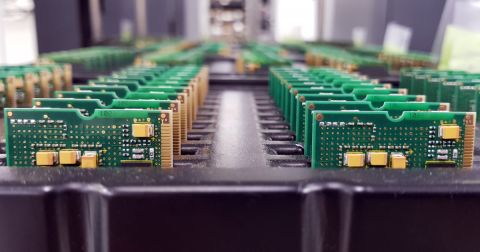
Small components on a PCB
Test Points
DFM includes test points for all important signals to check the electrical connectivity after building the board. If excluded, it will be difficult to check the final product. Here are a few pointers to avoid possible manufacturing issues:
- For ease of testing, place all test points on the same side of the board.
- Keep a minimum distance of 0.100 inches between the test points to increase the test effectiveness.
- Designate the area for taller components.
- Circulate all the test points evenly for easy access with multiple probes.
- Design your layout keeping manufacturing tolerances in mind.
Vias and Drill-to-Copper
Drill-to-copper is the distance from the edge of a drilled hole to the nearest copper feature. But PCB designers consider drill-to-copper from the finished hole size (FHS) to the nearest copper feature.
Designers should always consider the drilled diameter (FHS + drill tolerance) to determine the correct distance. The drilling diameter can be determined from the below equation:
Finished hole size + tolerance = drill diameter
Normally, the distance should be 5-8 mils but it depends upon the layer count. Board layout tools do not have any particular design rule checks (DRCs) for drill-to-copper. However, if you use adequate spacing in your design, you can have a clearance of 8 mils. This is the most important attribute to consider while doing DFM analysis.

Drill-to-copper clearance
In annular rings, tangency or breakout can occur when the drill bit fails to reach the desired spot and shifts away in the same axis. This causes marginal interconnections and affects reliability.

Annular ring breakout
Here are a few tips to avoid DFM problems that occur during drilling:
- Incorporate wide annular ring areas in your design by adapting bigger pad sizes. It ensures good conductivity and ease of drilling vias in the middle of the pad.
- Verify whether the plated drills have copper pads on all copper layers.
- Sierra Circuits recommends minimum 8 mils of drill-to-copper.
- Maintain a minimum aspect ratio to prevent misregistration of the drill.
- Define the drill type (PTH/NPTH) and drill count/size.
- Make sure the copper features and drills fit inside the profile of the board.
- Design an annular ring greater than or equal to the minimum annular ring size (4 mils) that can be manufactured by the vendor/fab house.
- Add teardrops to prevent annular ring breakout in complex designs and smaller annular rings.
Number of Drills Should Match the Drill Chart
It is crucial to match the number of drills with the drill chart. A drill chart is included in the fab drawing. Sometimes the drill chart doesn’t match with the actual drill count. In that case, you will need to modify or regenerate the drill chart.

Example drill chart PCB
As a simple design point, try to minimize the number of different drill sizes used in the PCB layout. It’s best to pick one or two via sizes that can handle most of the layer transitions for signals, and possibly a few others that will be used for mounting holes or non-plated holes.
Clearances
There are three types of clearances to observe in DFM analysis.
Edge clearance:
Many designers forget to provide adequate clearance between copper and the edge of the PCB. The proximity of copper to the edge can create shorts between adjacent layers if the current is applied to them. This is a result of exposed copper around the perimeter of the board. It is possible to resolve this problem by adding clearance to the design. Check the following approximations:
- For outer layer: 0.010”
- For inner layer: 0.015”
Line spacing:
Line spacing is the minimum distance between two conductors. It depends on materials, copper weight, temperature variations, and applied voltage. It also depends upon the capabilities of the manufacturer.

Solder mask clearances:
- Keep solder mask clearance greater than solder pads, except in the case of solder maskdefined pads.
- The best way to prevent solder bridges is to extend the mask opening onto the copper pad or provide barrel relief (solder mask clearance = drill size + 3 mils).

Solder mask clearance
Acid Traps
Another DFM error to watch out for is an acid trap. A design that incorporates acute angles will attract acid concentrations to that area. This may result in over-etched traces and open circuits.

Avoid laying the traces coming to the pads at acute angles. Place the traces at 45° or 90° relative to the pads. Verify that none of the trace angles have created acid traps after routing the traces.
Silkscreen Checks
Silkscreen check involves the different attributes that will influence the DFM analysis and will prevent possible errors. Here are a few important guidelines:
Orientation: Silkscreen may sit on the pads, and this should be checked by running a DRC. Silkscreen could also overlap a via hole, although this is acceptable if the vias are tented. This can happen while rotating the text and adjusting the component reference designator marks. Trim the reference designator marks that go over pads and vias to prevent overlapping.

Make sure your silkscreen orientation is consistent
Line width and text height: We recommend a minimum line width of 4 mils and text height of 25 mils for easy readability. Always use standard colors and larger shapes for good representation. Typically, the size should be 35 mils (text height) and 5 mils (line width). If the board is not dense and there is sufficient space for large text use the following size:

In case the above specifications do not work for a medium density board, use the following size:

When the above size does not work, refer to the following: For a medium-density board:

Silkscreen printing method: Specific method influences many design parameters such as size, clearances, etc., and elements like pads, vias, and traces. Specify these according to manual silkscreen printing, liquid photo imaging, and direct legend printing.overlapping.
Prioritizing markings: Prioritize the silkscreen marking as per the classification: regulatory requirements, manufacturers identification, assembly aids, and testing aids.
Following design for manufacturability guidelines help you recognize errors in the early design stage. Fortunately, the DRC engine in Altium Designer® can help you catch these problems before you go to production. After you consult with your manufacturer, you can program the constraints listed above into your PCB design rules to ensure you can quickly catch and correct errors. Once your design is ready for a thorough design review and manufacturing, your team can share and collaborate in real time through the Altium 365™ platform. Design teams can use Altium 365 to share manufacturing data and test results, and design changes can be shared through a secure cloud platform and in Altium Designer.
DFA Guidelines for an Efficient PCB Design
Every PCB that wants to become a real device will need to be assembled with high yield. Some strategic planning is needed to ensure the board can be assembled correctly on the first go. An understanding of some basic DFA guidelines can help ensure your design passes through manufacturing assembly with minimal defects and no rework.
DFA is a process that consists of three stages. In the first stage, the design of the board layout is taken into consideration. During this stage, clearance between components, the direction of soldering, and cost reduction for assembly are taken into account. In the subsequent stage, Gerbers or ODB++ files are validated for clearances and orientation of components, footprints, and various cleaning methods. In the final stage, wave soldering, reflow soldering, and manual soldering requirements are identified.

Objectives of DFA
Standardization
Every board designer will have a hard time forecasting the challenges that could arise while working on a new PCB design. The main objective of standardization is to minimize the level of uncertainty by using parts and techniques that have worked previously. Below are a couple of ways to ensure maximum standardization in your design:
- Validate each component’s source carefully to ensure the authenticity of the components. Unauthorized sources increase the risk of delays, misinformation, and counterfeit parts.
- Try to reduce the number of unique component packages to ease the design for assembly process and minimize potential errors. For example, if there are any footprint-to-land pattern discrepancies, the necessary layout adjustments will be accomplished more rapidly since the design will have fewer unique land patterns.
Component Validation
Every board designer will have a hard time forecasting the challenges that could arise while working on a new PCB design. The main objective of standardization is to minimize the level of uncertainty by using parts and techniques that have worked previously. Below are a couple of ways to ensure maximum standardization in your design:
One of the primary objectives of DFA is to validate components that go on the board. Follow the guidelines mentioned below to help your manufacturer to efficiently assemble your board:

Reducing Assembly Errors
DFA mainly focuses on eliminating potential assembly errors that may occur. Apart from the points discussed above, the below points enable manufacturers to fabricate circuit boards with desired functionality.
- Stick to size, spacing, and tolerances for drilled holes that fall within your fabricator’s capabilities. This also ensures the manufacturability of your PCB design.
- Follow clearances and tolerances that are within the capabilities of your CM.
- Follow board edge clearance rules.
- Ensure the board shape allows optimal panelization.
- Incorporate thermal reliefs where necessary.
DFA standards
As discussed in the previous sections, knowing the DFA standards helps you to design a board in an efficient and cost-effective manner. In this section, we will take you through a few critical DFA norms.
Component Orientation With Polarity Markings
Component orientation is one of the most important factors to be considered during the preassembly stage. For a hassle-free assembly, it is essential to follow clear and explicit techniques of orientation. Just as an example, consider diodes, which will have some definite polarity. Make sure the schematic symbol and silkscreen have a proper polarity marking that will be visible after placement. This will make the inspection process easier, and it makes testing or debug easier.

The symbol can be positioned between the two pins for through-hole parts, but it should be placed beside the device for surface-mount parts. Since these symbols can take up a lot of space, a bar above the cathode pad or a simple indication of A (anode) or K (cathode) would suffice for HDI boards.
Always group similar components and try to place them with the same orientation if possible. This facilitates a quick assembly process. For instance, all QFPs can be placed in a row with pin 1 at the same corner for each IC.

Spacing Requirements
Spacing between the components affects the time frame requirements of the PCBA process. In this section, we will have a look at recommended spacing standards to ensure the quality of the assembly process.
Part-to-Edge Spacing
Part-to-edge spacing is the distance from a given component on the board to its edge. This factor plays an important role during depanelization. During this process, the components near the board edge will be subjected to stress that might affect solder joints. We recommend a 125 mil clearance between the board edge and the SMD placed on the top side of the circuit board, but your fabricator might provide different allowances in their process.
Sometimes, manufacturers further increase the component-to-board edge spacing on the lower side of the board. This reduces the possibility of SMT component damage during the application of solder paste.
Copper traces can also be routed closer to the edge of the board. This allows a solder mask gap and prevents pad encroachment. Traces, copper pour, and manually inserted parts must be spaced at least 10 mils from the board’s edge. Castellated holes are a type of design that requires copper plating at the board edge. To achieve the desired copper plating, such designs will require additional expense and lead time.

Part-to-Hole Spacing
Spacing between the components affects the time frame requirements of the PCBA process. In this section, we will have a look at recommended spacing standards to ensure the quality of the assembly process.
- Part-to-hole wall: This is measured from the actual hole edge to the pad
- edge. This is also known as drill-tocopper distance. The minimum spacing required is around 8 mils.
- Part-to-annular ring: This is measured from the edge of the hole’s annular ring to the pad edge. The minimum spacing required is around 7 mils.

Part-to-hole spacing
IPC assembly standards
Here are some of the other IPC assembly standards your CM will stick to while assembling boards.
- IPC-A-600: IPC-A-600, commonly known as IPC-600, specifies the level of acceptance criteria for each product category. It defines the desirable, permissible, and non-negotiable requirements of the boards.
- IPC/WHMA-A-620C: It describes the standard for materials, procedures, tests, and acceptability criteria for cable and harness assemblies.
- IPC-A-630: It defines the standards for electronic enclosures. This standard is employed when your CM assembles and carries out the inspection process.
Common Assembly Defects
This section details the defects and issues that occur most frequently during PCBA. Manufacturers employ many quality control methods to avoid these defects, and some of those methods are mentioned in the subsections below.
Tombstones
A tombstone, also known as the Manhattan effect, refers to the case where an SMD component is partially or entirely peeled off of its landing pad. This is most common in small SMD passives (0603 or smaller packages) and it occurs due to force imbalances during reflow soldering.
Ways to prevent tombstoning:
- Ensure high component accuracy and a high preheat temperature.
- Avoid exposures to high temperatures and humidity.
- Extend the soak zone to balance the wetting force on both pads before the paste reaches the molten state.

Solder Bridging
Solder bridging occurs when the solder is applied between two conductors that should not be electrically connected. These undesired connections are referred to as shorts.
Ways to prevent solder bridges:
- Ensure high component accuracy and a high preheat temperature.
- Avoid exposures to high temperatures and humidity.
- Extend the soak zone to balance the wetting force on both pads before the paste reaches the molten state.

Solder Voids
Empty spaces or holes inside the solder joint are known as solder voids. A solder void is created when there isn’t enough solder available to establish a connection. Solder void typically consists of air.
Ways to prevent solder voiding:
- Increase the outgassing channel, allowing gasses to escape from the board.
- Try to use lead-free solder paste.

Inspection Methods
Once the circuit board is populated, manufacturers may perform multiple inspection and quality control procedures.
Automated optical inspection (AOI)
Automated optical inspection (AOI) is an efficient and accurate method for detecting PCB assembly errors before boards leave the production facility. This method employs highresolution cameras and advanced image processing software to identify assembly errors such as missing or misplaced components, solder bridges, solder balls, or tombstones.

X-ray Inspection
AXI (automated X-ray inspection) is a popular approach for detecting hidden defects in ICs and BGAs. The scanning source in this system is an X-ray. It can be used to identify huge voids and fractures. This approach allows non-destructive access to interior geometries and structural compositions. AXI captures images in the same way as AOI. The only difference is that AOI scans with a light source, whereas AXI scans with an X-ray.

2D X-ray inspection image
DFA guidelines are intended to ensure high yield and minimal rework after assembly. You can implement these and many other DFA guidelines before you go to production by using the DRC engine in Altium Designer®. After you consult with your manufacturer, you can program the constraints listed above into your PCB design rules to ensure you can quickly catch and correct errors. Once your design is ready for a thorough design review and manufacturing, your team can share and collaborate in real time through the Altium 365™ platform. Design teams can use Altium 365 to share manufacturing data and test results, and design changes can be shared through a secure cloud platform and in Altium Designer.
Communicating PCB Layer Stackup Needs to Manufacturers
In the business of PCB design, communicating needs to manufacturers and vendors is a top priority. The context of our requests is sometimes lost either by not providing the correct information, not listing enough information, or not giving any information. Although the experienced PCB designer can take steps to specify everything they want to see in their PCB stackup, eventaully the manufacturer will handle that decision in an effort to balance available materials with processing capabilities and yield.
Stackups describe more than the basic construction of the PCB; built into the stackup are many other design considerations defined by the material properties of your core and dielectric materials. To ensure your design is compatible with your fabricator’s capabilities, material stocks, and impedance requirements, designers have to make sure their stackup requirements are clearly defined. If you follow my advice when initially creating the design, and you initially ask your fabricator what stackups they have available, then you’ll be in good shape. If you design around that layer stack, then working with your fabricator will be much easier.
What if you have an existing design, and you need to get it produced anywhere with compatible material sets? How can you reduce the risk that the board you receive does not hit your requirements? That’s what we’ll look at in this article. If you follow some of these tips, you’ll be designing WITH manufacturing, not just designing FOR manufacturing.
Ensure PCB Layer Stackup Needs Are Specified
As I mentioned above, on the initial iteration of a design, it’s typically the case that you can obtain a standard stackup and use that in your design. This is the fastest way to get your prototype designed and put into production. The other option is to at least design your own stackup with materials you select, and then qualify this with your fabrication house. They’ll tell you whether or not they can produce it, and you can decide how to proceed from there (either redesign the stackup, or send it somewhere else).
When the design is already finishsed, it’s a bit of a different story. When you go to produce the design, you have to ensure the bare board fabricator can hit multiple specifications, including:
- Layer characteristics - This includes layer thicknesses, copper weight, copper foil type (reverse treated, electrodeposited, rolled copper, additive, etc.), and laminate construction/weave style.
- Dielectric and impedance requirements - If you have an impedance specification (both for signals and power) you need to hit, then you need to specify the dielectric constant in your layers along with layer thicknesses and copper.
- Allowed substitutions and tolerances - This is where your fabricator can see what you’ve given them permission to modify in order to ensure the design can be reliably produced anywhere.
We don’t often talk about Point #3 and instead focus of DFM as part of Points #1 and #2. If you can account for possible changes needed in your PCB layer stackup in Point #3, you can eliminate the risk that you receive boards that don’t hit your specs.
Just to ensure your PCB stackup needs are met, you have an important document you can use to specify your circuit board requirements: your PCB fabrication drawing. You’ll want to use both a stackup drawing and your fabrication notes to communicate your PCB layer stackup requirements to your manufacturer.
Start With a PCB Layer Stackup Drawing or Table
Inside your fabrication drawing, you can immediately specify most of the requirements for your stackup with a layer stackup drawing. This is the simplest way to give your fabrication house the basic requirements you want to see in your board. The example below is a design for a 4-layer board that could be used for a high speed PCB, power regulator module, microcontroller board, or another general-purpose board.

Example PCB layer stackup drawing in a fabrication drawing. This was created in Draftsman.
Example PCB layer stackup drawing in a fabrication drawing. This was created in Draftsman. From this drawing, we can already see several important specifications that your fabrication house will need to meet:
- Layer thickness and count
- Copper weight on each layer
- Specific material set (ITEQ IT-180BS/IT180C in this case)
- Gerber file extension matching each layer
Sometimes, when I receive requirements lists from clients, these points will be compiled into a stackup document. When submitting your design outputs to your manufacturer, it’s fine to include a stackup document or other requirements document as part of the file package, but this information should also be reflected in a fabrication drawing. The best way to do this is with a stackup drawing as shown above.
What about impedance and dielectric properties? If you’re designing with a specific material set in mind, then you don’t need to list these explicitly, although these can be included in your PCB layer stackup drawing. To ensure your fabrication house is accounting for these tolerances in your design, you will have to specify acceptable tolerances on trace widths and layer thicknesses.
Tolerances in Your Stackup and Trace Widths
To ensure you hit a dielectric constant target, thermal/chemical property target, or an impedance target (assuming you’ve specified this), there are three ways to proceed in your design:
- Before doing any design work, get your stackup approved by your fabrication house. If they approve it, make sure they specify a trace width for your impedance value based on controlled impedance data. If you design around this trace width and layer stack, then you’ll know the specifications you provide in your fabrication drawing will produce the desired electrical behavior.
- Specify the IPC slash sheet conformance for any compatible materials that will be used in the PCB stackup. You need to know a desired slash sheet for an initial material selection. • Allow the fabricator to adjust trace widths as needed in order to accommodate any
- Allow the fabricator to adjust trace widths as needed in order to accommodate any material swap used in the PCB stackup. You don’ need to specify a specific slash sheet or material name, although you’re free to do so in your fabrication notes.
Option #1 ensures your board will be accurate, but only at fabricators that offer only your specific material set. Options #2 and #3 are more general, and they attempt to cover you everywhere, but you may have to request impedance controlled testing implemented during fabrication.
Implementing Option #2 is simple in your fabrication notes. The image below shows an example fabrication note that states clearly which slash sheet your material set must conform to (note 16.C, outlined in red). Note that this can be implmented even if impedance control is not needed.

This fabrication note specifies slash sheet conformance so that the fabricator only swaps with compatible material sets.
Within Option #3, your fabrication house may need to adjust these specifications a bit. You will need to specify allowable tolerances on layer thickness and trace width in your fabrication notes. The example below shows how this can be specified as an allowable tolerance for the fabrication house. The red box defines the nominal impedance target implemented in the design as it is initially supplied to the fabrication house. The blue box specifies the allowed tolerances on the trace width and layer thickness

These two fabrication notes allow the fabricator to adjust the trace or layer geometry so that an impedance target can be hit within the tolerance specified in Note 18.A.
By doing this, you’re accounting for the fact that the materials a fabrication house uses may have different dielectric constant than what you used in your design. Because they won’t always be able to hit the required dielectric constant, they will have to adjust the trace to compensate for any major difference that brings the impedance outside the specification defined in Note 18.A.
When you’re ready to compile documentation for your PCB design and send your manufacturing file package into production, use the autoamted drawing tools in the Draftsman package included in Altium Designer®. Once you’re ready to release your fabrication data to your manufacturer, you can easily share and collaborate on your designs through the Altium 365™ platform. Everything you need to design and produce advanced electronics can be found in one software package.
What Solder Mask Expansion Value Should You Use?
The solder stop mask layer caps off the PCB and provides a protective film over copper on the surface layers. Solder mask needs to be pulled back from landing pads on the surface layer so that you have a surface where components can be mounted and soldered. This removal of the solder mask from a pad on the top layer should extend some distance around the edge of the pad, creating either NSMD or SMD pads for your components.
How far back should you pull the solder stop mask expansion so that you can prevent an assembly defect and ensure there is plenty of area for soldering? As it turns out, with steadily smaller components and higher density layouts being the norm, solder mask expansion can create small solder mask slivers that will be leftover on the surface layer. At some point, the minimum allowable solder mask sliver and the required solder mask expansion become competitive design rules; you might not be able to satisfy both rules simultaneously.
Balancing Solder Mask Expansion and Slivers
Perimeter Pad Size vs. Misregistration Tolerance
This is the primary reason to apply a positive solder stop mask expansion, which creates a nonsolder mask defined (NSMD) pad. The justification for this has to do with the copper etching process; copper etching being a wet chemical process, actually has higher precision than solder mask application. Thus to ensure the entire pad area is always exposed, we apply a sufficiently large solder mask expansion around the pad.
The lower precision of the solder resist application process can create misregistration, where the solder stop mask does not perfectly match the location where it is defined in your PCB layout. However, if the solder mask expansion is large enough, it will compensate for the misregistration and the pad can still be fully visible through the solder mask. The smallest recommendation on solder mask expansion recommendation I’ve seen is 3 mils on all sides of the pad, which will compensate for misregistration of approximately 2 mils.

This pad has a small amount of solder stop mask misregistration.
What if your pads are already sufficiently large? In that case, you could justify going with a smaller solder mask expansion value. In this case, if you use a smaller expansion with larger pads, you’re still assured to have sufficiently large exposed pad area even if there is some misregistration. In any case, you also have to consider the need for solder dams between nearby pads/vias.
Minimum Solder Dam Size
The minimum solder resist sliver size will limit the solder stop mask expansion opening you can apply for a given lead pitch. If the lead pitch is large enough, then you can always apply a large solder mask expansion without worrying about hitting a solder dam limit. When the lead pitch gets small, or when components get packed close together, you might violate the minimum solder mask sliver size. In that case, you need to decide whether you favor compensating for misregistration or ensuring there is always some solder dam. On fine-pitch components, I prefer the latter.

These locations will violate mode fabricator limitations on minimum solder dam size. Assembly defects could be prevented by applying some extra spacing between the pads for different components.
Because the solder stop mask web needs to be at least approximately 3 mils to stick to the surface of a PCB substrate, you can generally fit minimal solder mask expansion around a pad when the pad pitch is 20 mils or higher. If you’re looking at internal leads (such as inner balls on a BGA footprint), it’s appropriate to use SMD pads and place small dams between pads and vias.
Should You Let Your Fabrication House Decide?
If you just set a blanket design rule and apply 0 mil or 1 mil expansion so that you can hit your density requirement, your fabricator might apply an additional expansion value. If they do this, they might not tell you about it; you should expect that a fab house might apply this to overcome misregistration between the solder stop mask stencil and the pads on the surface layer.
My preference has been to set the mask to 0 mil on most projects for two reasons:
- Unless I’m dealing with a very high density layout, the footprints we’re using for most components will have large enough pads that the typical amount of misregistration won’t significantly reduce the soldering area on the pad.
- I already know the fabricator will increase the solder mask expansion because I work with a limited number of fabrication houses; I know their process and I’ll get a chance to check exactly what they want to modify when they send me their DFM report.
Point #2 should illustrate the reason you should have a preferred set of fabrication/assembly companies you use, and you should understand their process. My company has several manufacturing partners that we use exclusively for low and mid-volume client projects. We know what they expect and the feedback we might receive after an initial DFM/DFA review.
If you want to really communicate your intentions to your fabricator, make your intentions clear in your fabrication drawing. Add a note to your fabrication drawing that states the fabricator has permission to modify solder resist openings within a certain range (maybe +/- 3 mils). The other option is to put a specified tolerance on your solder mask expansion, and then specify a minimum sliver width. Just note that they might send the board back to you if your tolerance is too tight, at which point you might need to relax your tolerance requirement.

Note 10 in these fabrication notes specify what level of solder mask expansion I’m willing to tolerate in this design. In this case, I’ve specified that I prefer solder mask openings to match the pad size.
Once you’ve determined the minimum solder mask expansion and sliver you need to prevent assembly problems, you can use the CAD tools in Altium Designer® to define your land patterns and footprints. You and your team will be able to stay productive and collaborate efficiently on advanced electronics designs through the Altium 365™ platform. Everything you need to design and produce advanced electronics can be found in one software package.
Is It Printed or a Component? All About PCB Test Points
Test points in your electronic assembly will give you a location to access components and take important measurements to verify functionality. If you’ve never used a test point or you’re not sure if you need test points, keep reading to see what options you have for test point usage in your PCB layout.
PCB Test Points as Components and Printed Elements
Very simply, PCB test points can be intentionally placed as printed elements in a design, such as a bare pad or a via with a connection to an internal trace/plane. These can then be accessed with a test fixture during electrical testing, such as basic electrical (continuity) testing, in-circuit testing, or a fixture-les flying probe test. Even if you do not intentionally place test points as pads or other fixtures in your PCB layout, you can still define specific conductors as test points.
Does every design need test points? Not necessarily; for a prototype, you’re better off taking the time to do functional testing by hand so that you can more easily identify any failures. You’ll be able to see and touch the boards and instruments you’re working with, so it will be much easier to identify problems during testing. If you’re scaling in any way and you’ve thoroughly evaluated your testing requirements, then it’s best to place test points for in-circuit or functional testing with your manufacturer, this way they can automate those basic functional tests on the line.
As far as what are test points, they can be placed as components, pads, vias, or other printed elements in your board. Test points can also be tagged for access during fabrication or assembly in your design software. Now, let’s look at some of the options you have for test points in your PCB layout.
Test Point Pads and Vias
One thing you can do is intentionally place a pad along an interconnect or somewhere on a bus as a test point. You could also place this as a via so that inner layers could be easily accessed. These could be placed along a trace (in series) or off to the side as a small stub. For low-speed digital and lowfrequency analog (even if it is impedance controlled, this will not be a signal integrity problem. More specialized testing with highspeed/high-frequency signals will need a specific test structure with controlled and matched impedances at each port; keep this in mind before going and placing test points over every interconnect.

It’s common to place an array of test points around a large processor so that important nets (PWR, GND, configuration, etc.) can be accessed during testing.
Test Point Components
Some companies manufacture and sell test point components that can be mounted directly on your PCB. An example from Keystone is shown below. This component will be defined in your schematic as a 2-terminal component and placed in the layout just like any other through-hole component. SMD components are also available.

Example test point (Keystone 5001)
These components are great for attaching a probe to take measurements of a waveform. Note that these only have one connection point. If you’ve connected this test point in series with the target interconnect, you can use this component to measure the voltage waveform on the target interconnect (i.e., with an oscilloscope). At low-to-moderate frequencies (below 1 GHz) and rise times (above 10-20 ns), you can use a direct connection with your probe to take your measurement, and you won’t have to worry about test point impedance or reflections as long as the frequency is low enough. This makes these components good for accessing important waveforms like motor drive, low frequency analog, slower digital buses (I2C or SPI, for example), or GPIOs on your MCU during functional testing.
Mix and Match
In general, you can mix and match different types of test points depending on your needs. Best practices would dictate placing a test point component or specific test f ixture on the board if you need to access an interconnect or waveform during functional testing. Otherwise, for in-circuit testing, flying probe tests, or continuity testing, you should place pads or vias to touch specific points in your board. Test points that aren’t placed as specific pads or fixtures are normally defined on specific vias, component pads, power/GND connections, or other exposed conductors on the fabricated PCB.

Test point components can be placed on the same board as test points for fab or assembly.
More Specialized Testing
What we’ve shown here is intended for in-circuit testing during fabrication/assembly, as well as testing the PCB with a probe to look at a waveform or level. For something more specialized, like a highly accurate impedance measurement or impulse response measurement, simple PCB testpoints with a simple conductor connection (either mechanically fixed or soldered) might not give you the results you expect. More sophisticated test fixtures are needed to connect your PCB test point access to your signal generator or analyzer. One example is the 2x-thru design as specified in the IEEE P370 standard.
Oftentimes, when a specialized interconnect is being designed for use in a high frequency or high speed system, the strategy is to build a test board that holds the interconnect and its connectors. If you specify controlled impedance for your fabricator, they will not test specialized interconnect designs (such as a waveguide) as they won’t have a test coupon that has your specific interconnect. Standard transmission line types are fine, but something more specialized requires you to build the test coupon yourself, or you provide the design files for the test coupon to your PCB fabrication house so that they can test it.
For some low-impedance PDN measurements with short impulses or frequency scans below about 10 GHz, you can just use coaxial connections to test probes that touch your PCB test point pads to make a low impedance connection. If you’re doing frequency domain measurements to get network parameters, be mindful of error sources related to your reference selection. I’ve covered this elsewhere in regards to power integrity, as have other experts who specialize in low-impedance S-parameter measurements.
When you need to place a PCB test point as a printed element, probe connection, or a specialized test fixture, use the complete set of design features in Altium Designer®. The complete set of test point management tools and the Draftsman utility can help you specify your test point and performance requirements for your product. When you’ve finished your design, and you want to release files to your manufacturer, the Altium 365™ platform makes it easy to collaborate and share your projects.
ABOUT ALTIUM
Altium LLC (ASX: ALU) is a multinational software corporation headquartered in San Diego, California, that focuses on electronics design systems for 3D PCB design and embedded system development. Altium products are found everywhere from world leading electronic design teams to the grassroots electronic design community.
With a unique range of technologies Altium helps organisations and design communities to innovate, collaborate and create connected products while remaining on-time and onbudget. Products provided are Altium Designer®, Altium Vault®, CircuitStudio®, PCBWorks®, CircuitMaker®, Octopart®, Ciiva® and the TASKING® range of embedded software compilers.
Founded in 1985, Altium has offices worldwide, with US locations in San Diego, Boston and New York City, European locations in Karlsruhe, Amersfoort, Kiev and Zug and Asia-Pacific locations in Shanghai, Tokyo and Sydney. For more information, visit www.altium.com. You can also follow and engage with Altium via Facebook, Twitter and YouTube.

About Author
Related Resources
Table of Contents
- Complete Guide to DFM Analysis
- What Goes Into DFM Analysis for PCBs?
- Inspect Your Design Often
- Component Clearances
- Looking at Footprints
- Stackup Check
- DFM Analysis Before Fabrication
- Checking Feature Sizes Against Process Capabilities
- IPC Class Compliance Review
- How to Get Your Design Data to Your Fabricator Quickly
- Preventing Top DFM Errors in Your PCB Design
- Preventing Top DFM Errors in Your PCB Design
- Top DFM Errors
- Prevention of Slivers
- Component Selection
Design to Release, Without the Friction
- Keep reviews tied to the right version
- Reduce handoff confusion and rework
- Spot sourcing and release risk earlier
- Work solo, share when needed
Get Started
Thank you, you are now subscribed to updates.

