


Tips for Managing the Hardware Development Cycle

At a Glance
Optimize collaboration, reduce redesigns, and streamline your hardware development cycle. Learn essential tips for managing PCB design projects efficiently.


PCB design is like a wonderful puzzle, but each hardware development cycle can be complex and involve multiple collaborators. Here’s how you can take control of the process.
When I get started with a new project, I know it’s time to get everybody on my team on the same page as to board requirements and overall platform requirements. A lot of what we do these days is more than just layout; we’ve had to take on embedded firmware, supervising manufacturing, and interfacing directly with end customers to ensure project requirements are being met. Everyone involved needs access to the same set of design data (including code!) to measure progress throughout a project.
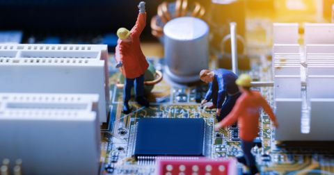
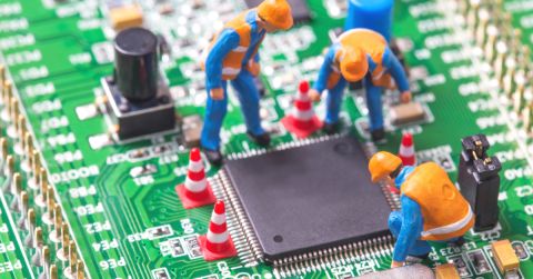
If you want to get through a hardware development cycle without redesigns or failed board runs, it’s all about how you collaborate, especially if you work on a remote PCB design team. Here are some simple management and collaboration strategies you should follow to help you get through design cycles successfully.
The Hardware Development Cycle for PCBs
Getting through the hardware development cycle and successfully managing a project to completion is no easy task, especially when working with a remote team. Simpler projects can be farmed out to a contractor or an individual designer, but complex projects require a lot of work for the project to be successful.
A typical hardware development cycle is shown below. Note that only one of these phases involves actual PCB design; two of these phases are all about gathering and analyzing requirements, and the last phase focuses on getting the product built and tested. Throughout the process, you’ll need to collaborate with multiple stakeholders to get a complex project completed successfully. Keep reading to see some tips for success in each of these areas.

Get Complete Requirements and Get Them Early
Perhaps the most important group in the product design process is your customers and end users. If you want a hardware development cycle to produce a useful product that works properly, you’ll need to gather their product requirements before you begin a design. This might sound like a simple task, but if you miss a simple product requirement, you might be setting yourself up for an extensive redesign.
Here are some areas where you should gather complete requirements from the end customer or user:
-
Desired technical specs. Things like battery lifetime/power consumption, signal integrity requirements, unique components or placement on the board, and even simple things like indicator LEDs or board size should be defined early. Classify these points into must-have and nice-to-have requirements.
-
Required components. The end customer or technical specs might dictate that you must use a specific component as your processor (e.g., specific MCU or SoC). If you know you’ll need these components, and you’ve verified they’re in stock, you can dig into the specs early and see where they’ll fit into the end product.
-
Platform requirements. If you’re developing an embedded system, you may need to gather a whole other set of requirements related to how your system needs to interface with a larger platform or application.
-
User experience. What will the end user of this product expect? This is an important question to ask as it will inform technical requirements. It may even reveal a new way to create the design, or it may require revisiting some technical specs. Again, classify user experience requirements as must-have or nice-to-have.
-
Extensibility. The software world is great at designing for extensibility because it is so easy to add new features to a piece of software. This isn’t always the case with hardware. Designing for extensibility means designing the system to accommodate additional features as they might be needed. Something as simple as placing additional switches, solderable jumpers, or headers on unused pins lets your end user make additional connections or modify the design in the future.

Sometimes, the end customer or user doesn’t know exactly what they want or need in their new product. I find that this happens when the end customer isn’t a hardware engineer, so communicating technical data to them isn’t so useful for getting the answers you need. Instead, communicate PCB design options to this group of stakeholders in terms of the end-user experience rather than what it means electrically. This helps the end user make firm decisions as to what they want in the end product.
After you’ve gathered the product and user experience requirements, it’s time to start putting together a real product in your PCB design tools. You’ve officially entered the design phase. Here are a few strategies I’ve found that help keep everyone productive and cut down on total design time.
Use Development Boards During Design
Whenever we have to create an embedded system with a central MCU/FPGA and multiple ICs, we always buy a development board for each component. These boards are precisely designed to support the components you need with minimal signal integrity problems. This provides an easy way to start programming the host controller and verifying whether different components in the system will produce the desired user experience.

Once you’ve qualified everything on development boards, it’s much easier to transfer your code over to a prototype and start working out any bugs in your finished system. This can also help your engineers develop functional testing requirements for a new product before engaging with a manufacturer.
Centralize Communication and Sharing
Since communication on the front end is so important in a successful hardware development cycle, your team and project stakeholders should use a centralized solution for communicating. Chat tools like Skype are great for quick chats and informal updates, but complex designs often need some questions or comments placed directly in the design data. These points can come from the designer, firmware engineer, customer, or manufacturer. Chats can get cluttered quickly, especially when you’re collaborating with a remote team.
When your design data can be accessed through a cloud collaboration solution, everyone involved in creating a new product gets visibility into the design process. Design teams that work remotely need to access a consistent set of PCB design data to stay productive and close the loop on hardware development cycles. This type of solution can only be found on a cloud platform that integrates with your design tools.
When you use Altium Designer combined with the Altium 365 platform, your team and stakeholders can be involved throughout a hardware development cycle. Altium 365 lets you bring end users and manufacturers into the process, which can help you get through a design review faster and avoid time-consuming redesigns. Everyone on your team will have access to supply chain data, commenting features, and data-sharing tools to help streamline PCB design collaboration.

About Author
Related Resources
Related Technical Documentation
Table of Contents
Design to Release, Without the Friction
- Keep reviews tied to the right version
- Reduce handoff confusion and rework
- Spot sourcing and release risk earlier
- Work solo, share when needed
Get Started
Thank you, you are now subscribed to updates.


