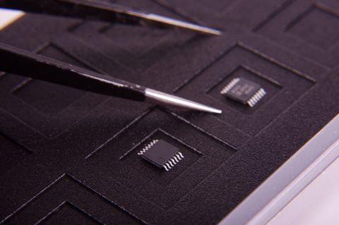
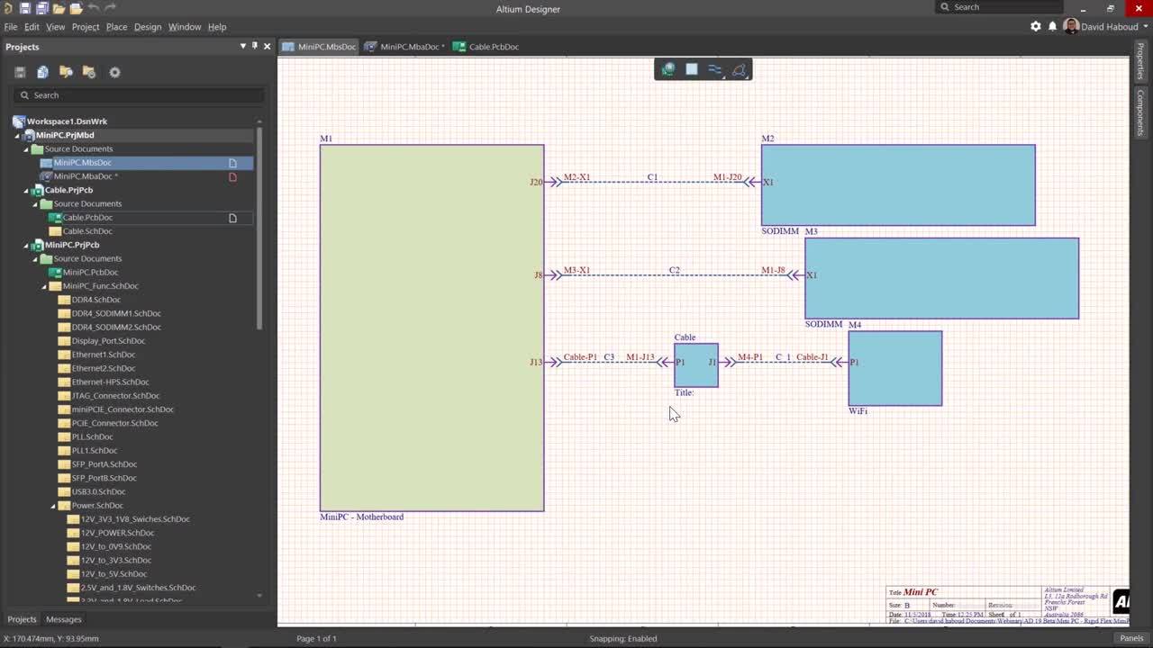
Создавайте многомодульные сборки с гибко-жесткими платами и одноплатными модулями.
This page takes a detailed look at Controlled Depth Drilling (CDD), also known as back drilling - a technique used to remove the unused portion, or stub, of copper barrel from a thru-hole in a printed circuit board
This page looks at the PCB Editor's support for embedded components - components that are manufactured as discrete entities and then placed on an inner layer of the circuit board during fabrication/assembly
This page looks at the PCB Editor's support for via stitching (used to tie together larger copper areas on different layers) and via shielding (used to help reduce crosstalk and electromagnetic interference in a route that is carrying an RF signal)
Explore Altium Designer 24 technical documentation for Analyzing Design Signal Integrity and related features.
This page describes the various options and settings that you configure in Altium Designer to successfully design your high-speed board
This page looks at the xSignals feature, which enables the correct treatment of a high-speed signal path as just that - a path for a signal to travel between a source and destination, through termination components as well as branches
This page takes a look at the functionality of Altium's PDN Analyzer extension, including its installation and licensing, power integrity essentials, and an overview of performing a power delivery network analysis
This page details the PDN Analyzer panel, which provides the user interface for the Altium Power Deliver Network (PDN) analysis tool, available as a purchasable Altium Extension application for Altium Designer
This page provides detailed examples of working with Altium's PDN Analyzer. Analysis basically involves setting up the PI-DC simulation net parameters, running the simulation and then interpreting the results. Data is drawn from the active PCB project
Explore Altium Designer 24 technical documentation for PCB Layout Replication and related features.