Silk to Solder Mask Clearance: The PCB Design Rule You Need to Add

I was impressed that, right out of the box, the stock design rule checks (DRCs) in my copy of Altium 20 pretty much covered all the bases on how to make a “standard” printed circuit board (PCB). Altium Designer defaults to “10 mil” rules, which means that the standard spacing and widths of copper tracks is 10 mils. What's more, most of the other spacings also default to 10 mils. This includes track to track, pads to tracks, through-holes to other pads or vias, and pretty much anything else you can imagine. The exceptions are the silk to solder mask clearance and the solder mask expansion clearance around pads, both of which default to 4 mils.
Starting a new design means selecting the PCB design rules that matter for your circuit boards. This set of rules is supported by PCB fabrication companies and they help engineers design a functional circuit board. Exceptions to the default 10 mil rules exist, especially as density and complexity increase. For example, entirely different sets of design rules may exist in regions such as the area under an Integrated Circuit (IC) with a Ball Grid Array (BGA) footprint.
As density increases and/or as signal edge rate increases, it is not uncommon for these rules to be listed in other units and levels of complexity.
PCB Design Rules Should Match Fab Capabilities
I tend to design for “6 mil rules”, as I turn quick little designs through PCB fabricators using online ordering procedures. When setting up for a new PCB, I will decide on the range of PCB fabs I want to use, as well as an estimation of PCB fabrication budget.
Once the ruleset and type of fab house is decided, the fabrication capabilities need to be examined and translated to rules or policies that Altium Designer can understand. Often I will create vendor-specific rulesets in addition to generic “x mil rule” rulesets that represent the capabilities of that vendor pretty much line by line, stat for stat.
Again as things get more complicated, we respond by adapting the rulesets and the compromises in fabrication that they represent. Understanding the fabrication process comes in handy in these instances. For example, the center of the board may have the best drill-to-copper registration where rules can be bent more. To think of it another way, in cases where rules need to be bent and fabrication capabilities pushed, it is best to statistically increase the chances of success wherever possible.
Aside from the typical conductor-to-conductor clearances defined as default design rules or in IPC standards, there are other clearances that should be considered when density needs to be increased without creating assembly defects. These clearances involve your solder mask (or "solder resist") and silk screen, which many designers will simply take using the default values. Instead, set up some custom values to ensure Altium Designer will not trigger unnecessary errors.
Solder Mask Sliver
If you're ever working with very high density designs and you start finding pad clearances are getting very tight, it makes sense to define areas where the remaining solder mask sliver between pads can simply be eliminated. If you have solder resist expansion defined around pads on your components, the remaining solder mask between pads will already be removed if the mask openings overlap. This helps you automatically remove remaining solder mask slivers that may be too small to be reliably fabricated.
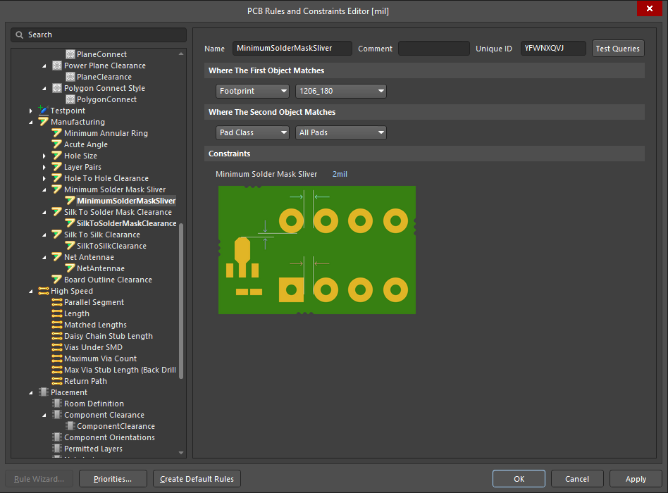
This rule gives you a simple way to manage solder stop mask slivers between specific pad classes, specific nets, and even specific footprints. As an example, in the above image, I've set a constraint on the minimum solder mask sliver between 1206 footprints and all pads. You could apply individual rules on different layers, between different pad classes, and much more.
Solder Mask Expansion
Another example of bending the rules is decreasing the solder mask expansion around high density pins and pads so that there is enough solder mask left between pins/pads to act as a solder dam and prevent solder bridges during assembly. This is clearly a tradeoff, as now there is less room for misregistration of the solder resist, which can affect solderability, or the likeliness of a solder bridge.
Solder stop mask expansion for a pad on a component can be defined when creating the PCB footprint and libraries. However, you can also set the solder mask to follow the PCB design rules; the value you set will be automatically applied to your components. The image below shows solder mask expansion being applied to every exposed conductor that is not a via on both layers. You could certainly apply different rules on the top and bottom layers.
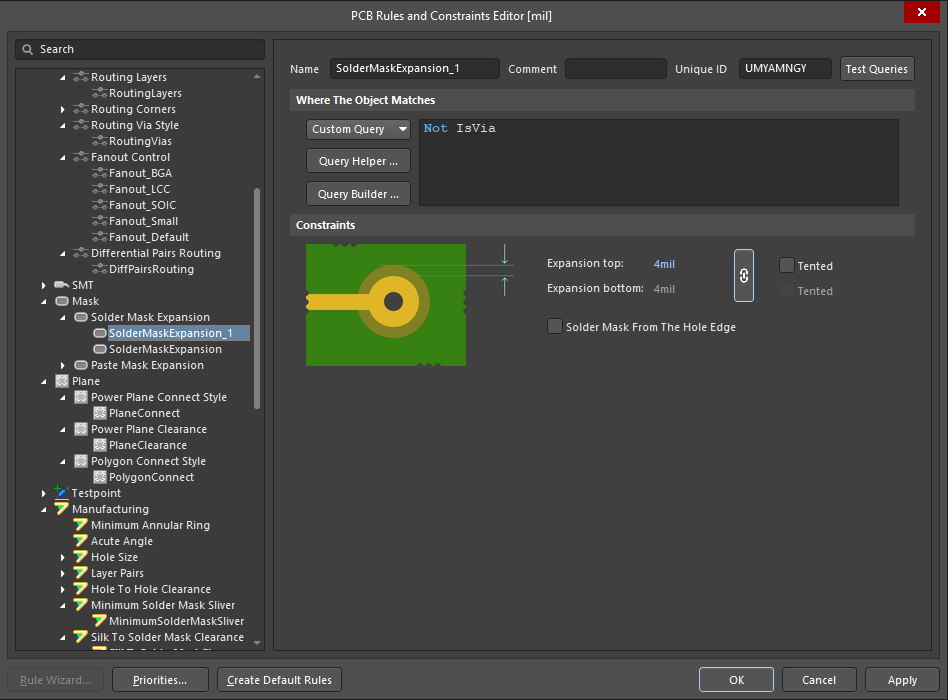
Just note that, if you want to set a specific solder resist opening for a specific component, it's easiest to do this in the PCB footprint. You can apply this to a specific pad on a component if desired. You could also set the rule for a specific ne, which would apply the solder mask expansion value to pad on that net.
Silk to Solder Mask Clearance
Some things we don’t have to worry about, sort of. If silk screen coincides with bare copper, the overlap will usually not be printed (it depends on the fab house); my fab houses tend to make bare copper bare. The result doesn’t usually harm the electrical function of the board, but the “silkscreened” text may be hard or impossible to read.
To further help you increase density in your designs and aid assembly, you can also modify the silk to solder mask clearance rule. The image below shows how you can define silk to solder stop mask clearances in the PCB Rules and Constraints Editor. Simply select the “Check Clearance To Exposed Copper” to define a minimum clearance to exposed copper elements like pads. To define a clearance to the edge of the solder mask opening, select the “Check Clearance To Solder Mask Openings” and set the desired clearance value.

In the above image, the silk to solder mask clearance is defined as 2 mil for the Top Overlay layer; simply create a second PCB design rule for silk to solder resist clearance if you want to add the rule to the Bottom Overlay. Note that this is only defined for pads (as given in the IsPad query), but we could also apply the rule to a pad class, pad class and layer simultaneously, or to all objects. This gives you the ability to balance what silk-to-object clearances you can accept in your design. The end result is that Altium Designer will generate a list of every instance in which the text overlaps bare copper on component pads.
Now if only someone would invent an automated function to move silk screened text off of exposed pads and vias across the board. >:/
When you need to design complex circuit boards with a comprehensive set of PCB design tools, try Altium Designer®. You can apply custom and standard PCB design rules for your next circuit board, including silk to solder mask clearance and other important fabrication rules. Would you like to find out more about how Altium can help you with your next PCB design? Talk to an expert at Altium and learn more about making design decisions with ease and confidence.


