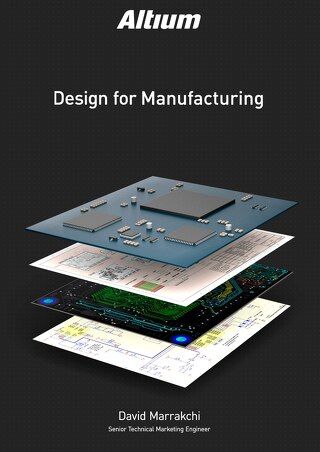
Design for Manufacturing Guidebook
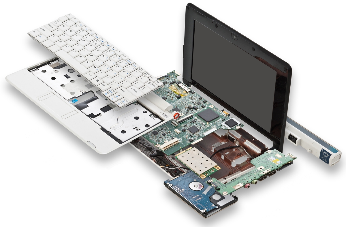
Design for manufacturing (DFM) isn’t just about your design process, it is about being aware of what happens both before and after you complete your board layout, from the first component you place digitally to the last part a pick-and-place machine places physically on your PCB. At its core, DFM is as much an art as it is a science, requiring engineers to be aware not only of their own cares and concerns in the design process but every stakeholder’s needs as well. It's a designer's responsiblity to understand the PCB manufacturing process so they can successfully implement DFM practices in their PCB.
In this guidebook, we've taken a deep look at DFM for PCB design from two perspectives: fabrication and assembly. In terms of fabrication, designers will be limited by processing capabilities and they must ensure that the physical layout in their system does not violate these constraints. In terms of assembly, the designer must still ensure their physical layout will not interfere with the basic aspects of the assembly process and will lead to high yields. To design a successful PCB right the first time, you need to look through a wider lens and see the design you produce in the digital domain as one small piece of a greater puzzle.
The goal in this guidebook is to give newer designers the tools they need to ensure they do not run afoul of DFM/DFA constraints within the PCB manufacturing process. We offer simple yet important guidelines on the following topics:
- An overview of the fabrication process
- Important elements to include in PCB footprints that will aid fabrication and assembly
- Important material properties that apply in material selection for most PCBs
- Tips for strategizing a PCB layout to ensure successful manufacturing
- Documenting your PCB using fabrication and assembly drawings
To learn more about other important PCB design topics, take a look at our Guide Books page on the Altium resources hub.

 Open as PDF

