HDI PCB Design
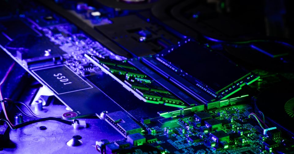
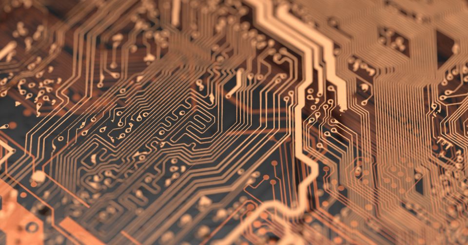
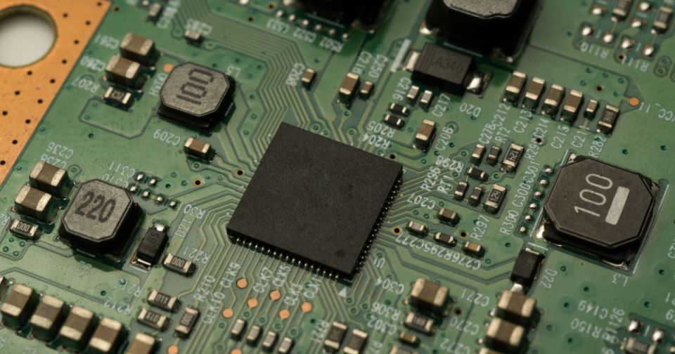
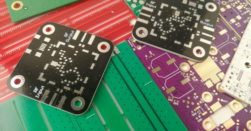
High density interconnect (HDI) designs push the limits of trace, via, and layer density. These boards have high layer counts with very small traces and vias. HDI PCBs also require different fabrication and assembly processes than typical circuit boards that use larger features. Browse our library of resources to learn more about implementation of HDI PCB design.
Guide Books
Explore Guidebooks for HDI Design and start creating today!


Videos
Watch videos for HDI Design to learn more!

Customer Success Stories
Discover customers finding success with Altium's HDI Design solutions!


Technical Documentation
Explore Technical Documentation related to HDI Design

Articles
Explore more popular content for HDI Design!