


What Is an Integrated Design Environment for Electronics?

At a Glance
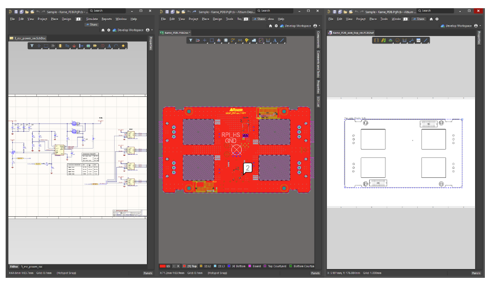
Discover how an integrated design environment unifies schematic capture, PCB layout, simulation, MCAD collaboration, and data management to prevent rework.


Late discovery of mechanical constraints is a common cause of schedule slips and rework in electronics projects.
Consider a typical scenario: three months into a design, the schematic is complete and the PCB layout is largely finished. Only then does the client mention that a second PCB is mounted a few millimeters above the main board, something they assumed was obvious from earlier photos. At that point, previously selected connectors and components are too tall, forcing reselection of parts that are already difficult to source due to voltage and current requirements. Several weeks of work are lost addressing a constraint that was never formally captured.
This type of issue is not unusual. It is a predictable outcome of disconnected design workflows.
Key Takeaways
- An integrated design environment combines schematic capture, PCB layout, simulation, MCAD collaboration, and data management so engineers are not forced to move between disconnected tools.
- Design rules and constraints (such as clearance, spacing, and component height) must be checked in real time during design, not after files are released for fabrication.
- Mechanical and firmware constraints must be introduced at the beginning of a project. Discovering them after component selection leads to unnecessary rework and delays.
The Problem: Six Tools to Build One Board
In many hardware teams, the design workflow is spread across multiple disconnected tools. Pad stack definitions may live in one application. Schematic symbols and libraries are managed in a separate tool and often stored in different local or network folders. PCB layout is handled elsewhere. System integration, signal integrity, and EMI analysis are typically performed in additional, specialized applications. Project tracking and task management are often web-based and not always accessible when engineers are working offline.
As a result, engineers must learn and maintain proficiency in at least five different tools just to take a design from schematic capture to a manufacturable PCB.
On small teams, this fragmentation creates additional overhead. Moving between tools requires frequent file exports and imports, with the risk of translation errors at each step. Libraries and footprints must be placed in specific directory structures to remain usable; a misplaced file can prevent a component from transferring correctly from schematic to layout.
Significant time is lost locating schematic symbols, PCB footprints, and the correct file versions, which is work that should be trivial but often consumes days or weeks over the course of a project.
Despite the number of tools involved, final coordination still relies on emails and spreadsheets. The tools themselves remain largely disconnected, providing little shared visibility across the design process.
What an Integrated Design Environment Actually Means
An integrated design environment for electronics is a single application, or a tightly coupled set of tools, that supports the full hardware design workflow:
- Schematic capture for circuit design
- PCB layout for component placement and routing
- Simulation for pre-fabrication validation
- ECAD-MCAD collaboration so electrical and mechanical teams work from the same data
- Data management for component libraries, project files, and design requirements
In an integrated environment, the same underlying data is used across all stages of design. Changes made in the schematic propagate directly to the PCB layout. Mechanical constraints, such as board outlines or enclosure clearances, are visible in the electrical design environment as they are updated.
This eliminates manual exports, file imports, and version mismatches that are common in toolchains built around disconnected applications.
- For a detailed explanation of how this works in practice between electrical and mechanical teams, see ECAD-MCAD collaboration in Altium Develop.
How Integration Closes the Feedback Loop
Here's a common scenario in a power electronics project. The PCB layout is created in one tool, schematic capture is handled in another, and the enclosure is designed separately in PTC Creo by the mechanical engineer. None of these environments share live design data.
In this case, the enclosure barely accommodated the PCB, and cable assemblies violated spacing requirements. These issues were not design errors in isolation. They occurred because no single environment provided visibility into the complete mechanical and electrical context. Resolving the conflicts required multiple back-and-forth cycles between electrical and mechanical teams and added two to three weeks to the schedule.
When ECAD and MCAD tools are integrated, this feedback loop closes. The mechanical engineer defines the board outline and constraints directly from the enclosure model, and those constraints propagate to the PCB layout. The electrical engineer immediately sees available board area, validated mounting hole locations, and component height limits before committing to part selection or routing decisions.
This bidirectional synchronization reduces iteration, prevents late-stage conflicts, and shortens overall design cycles.
- For additional details on ECAD-MCAD collaboration, see the MCAD CoDesigner documentation.
Real-Time Design Rule Validation Saves Your Boards
Return path vias, clearance violations, and design-for-fabrication or design-for-assembly spacing errors are common causes of PCB rework and respins. These issues often slip through when design rules are only checked after layout is complete.
Real-time design rule validation flags violations at the moment they are introduced. If a clearance constraint is violated, it is immediately visible. If a trace width does not meet the requirements of its assigned net class, the error is highlighted directly in the layout.
This approach differs from batch-based design rule checks, which identify issues only after the design work is complete. Batch checks reveal problems that may have been introduced hours or days earlier. Real-time checking prevents these errors from propagating by enforcing constraints during layout.
The Real Cost of "Fine"
“Our current toolchain works fine” often means the process is fragile.
In one project, schematic capture software was used for cable and harness design. While it was technically possible, the tool was not designed for that purpose. As a result, electrical changes did not propagate automatically to the drawings, and every label and text field had to be updated manually.
This created predictable failures. Several cable assemblies were built with incorrect wiring because the documentation was out of sync with the actual design. Engineers spent significant time reviewing, rechecking, and correcting errors that should have been prevented by the tool itself. Individual productivity dropped to an estimated 40-50% due to the constant overhead of manual updates and verification.
The system functioned, but only in the sense that it did not immediately fail. The real cost of “fine” was paid in rework, delays, and reduced engineering capacity.
When Firmware and Mechanical Show Up Late
On a recent project, the main PCB design was completed, the bill of materials finalized, and the design was ready to be released for fabrication.
At that point, a new constraint emerged: a secondary LED board would be mounted on top of the main board, with only 10 mm of vertical clearance.
This late requirement forced a redesign of the affected area. Existing connectors exceeded the allowable height. Components with sufficient current capacity were not available in low-profile packages. Alternative parts that met the height requirement had impractical minimum order quantities or were already obsolete.
Approximately four weeks were spent evaluating alternatives, resulting in $2,000 in additional consulting costs (roughly 10% of the project’s total budget) only to determine that the original design approach was not viable.
Compounding the issue, Chinese New Year shutdowns delayed fabrication. Boards that should have shipped in October or November were not delivered until March.
The root cause was not a technical failure, but a process failure. Mechanical constraints were not communicated at the start of the project, and there was no shared environment where electrical, mechanical, and firmware teams could view and validate system-level requirements early in the design cycle.
Why Everything Needs to Work Together
Software systems can often tolerate partial failure. If one function breaks, other parts of the application may continue to run, allowing issues to be fixed incrementally.
Hardware systems do not behave this way.
If the power architecture is incorrect, if level shifters are misapplied, or if fundamental interfaces fail, large portions of the board will not function, or the system may not power up at all. Hardware requires a high degree of correctness across all subsystems before meaningful testing can begin.
Because hardware is inherently integrated, the development process must be integrated as well. Requirements cannot live in email threads. Design rules cannot be checked only at the end of the layout process. Mechanical constraints cannot be discovered months into development without introducing rework and delay.
Design tools should reflect this reality. Electrical, mechanical, and component data must be connected, visible, and accessible throughout the design cycle, not managed as disconnected files and handoffs.
For teams ready to move past the disconnected toolchain, Altium Develop is a good starting point.
Whether you need to build reliable power electronics or advanced digital systems, Altium Develop unites every discipline into one collaborative force. Free from silos. Free from limits. It’s where engineers, designers, and innovators work as one to co-create without constraints. Experience Altium Develop today!
Frequently Asked Questions
What is an integrated design environment for electronics?
An integrated design environment brings schematic capture, PCB layout, simulation, ECAD-MCAD collaboration, and data management into a single, connected workflow. Instead of moving files between separate tools, engineers work from shared data so changes propagate automatically across design stages.
How does an integrated environment reduce rework and schedule delays?
By validating electrical, mechanical, and manufacturing constraints in real time, issues like clearance violations, component height limits, or routing conflicts are caught as they occur, not weeks later. This prevents late-stage redesigns that typically cause missed schedules and added cost.
Why is ECAD-MCAD integration critical early in a project?
Mechanical constraints such as enclosure geometry, board stacking, and connector alignment directly affect component selection and layout decisions. When these constraints are visible from the start, teams avoid choosing parts or architectures that later prove infeasible.
How is real-time design rule checking different from traditional batch checks?
Real-time checking flags errors immediately when a rule is violated, allowing engineers to correct issues before they propagate. Batch checks only identify problems after layout is complete, often requiring significant backtracking and rework.

About Author
Related Resources
Table of Contents
- Key Takeaways
- The Problem: Six Tools to Build One Board
- What an Integrated Design Environment Actually Means
- How Integration Closes the Feedback Loop
- Real-Time Design Rule Validation Saves Your Boards
- The Real Cost of "Fine"
- When Firmware and Mechanical Show Up Late
- Why Everything Needs to Work Together
- Frequently Asked Questions
Design to Release, Without the Friction
- Keep reviews tied to the right version
- Reduce handoff confusion and rework
- Spot sourcing and release risk earlier
- Work solo, share when needed
Get Started
Thank you, you are now subscribed to updates.