


Migration Guide Siemens Xpedition Enterprise to Altium Designer develop


Preparing to Migrate Your Legacy Data
Never forget that migration of data follows the “garbage in.... more garbage out” principle. So, we need to consider four distinct phases of the process, this is best shown in the flow diagram below:
1. Prepare original data
|
2. Export data
|
3. Import data
|
4. Post import
|
Step 1: Prepare Original Data - Pre-Translation Tidy Up
It is important to clean up and tidy your design within your legacy system before trying to export. We’ve put together a checklist to help you:
Schematic considerations:
-
Does the design have single pin components representing power objects?
-
Connectors are represented as one-gate-per-pin with over 256 “gates”
-
Keep a note of the ambiguous connectivity in the design (For example - multifunctional pins, hidden pins, or implicit connections)
-
Be sure to understand which nets in the design are local (defined at the document level)
-
Are the schematic symbols mapped to the correct PCB footprints?
-
Are the schematic and PCB synchronized?
PCB considerations:
- Make note if the design has star point earth connections
- A large number of graphical objects like mechanical drawings or non-ECO-registered drawing primitives need to be assigned in the documentation layers
- Deliberate DRC violations (for example, allowed short circuits and net-ties)
- Are there any objects extending beyond the environment?
- Knowledge of correct PCB layer assignment is required to map the imported layers with existing layers in Altium Designer Develop
- Do the auto-named nets match the schematic?
Library considerations:
- Schematic symbols match with PCB footprints
- Correct supply chain information and BoM parameters
- Associated 3D models cannot be imported for Siemens libraries, but you can import the respective STEP models in Altium Designer Develop later
- Correct representation of custom pads, copper shapes, solder mask and resist
Step 2: Export Data - Save Data in a Suitable Format
Supported Versions and File Formats
The following table details the versions of all xDxDesigner Schematic file types that can be migrated into Altium Designer Develop. Note that this list is updated when a major update is implemented for the Import Wizard. You can contact Altium’s Support team about specific systems and versions before undertaking migration.
| TYPE | SYSTEM | VERSION | FORMAT |
| Schematic | xDxDesigner | 7.9.4 | Database (.PRJ) |
| PCB | Xpedition | up to VX2.x | . pcb, .prj |
| Library | . lmc |
Altium Designer can import up to version 7.9.4 of xDxDesigner (Expedition Enterprise 7.9.4, or simply EE7.9.4). Altium’s Import Wizard can translate xDxDesigner Schematic data (.PRJ).
Step 3: Import Data into Altium
Translating xDxDesigner in Altium Designer Develop
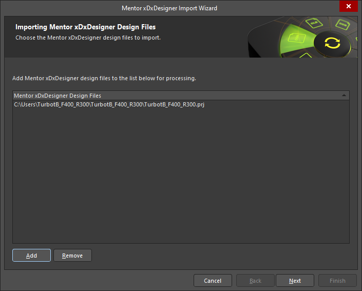
The Import Wizard can be launched from the Altium Designer Develop File menu. Choose the Mentor xDxDesigner Projects and Designs option as shown in the screenshot below. On the “Importing Mentor xDxDesigner Design Files” screen, click the Add button to choose xDxDesigner database files. Multiple files can be translated at the same time. Step-by-step instructions on using the Import Wizard follow next.
- Start the Import Wizard with File » Import Wizard
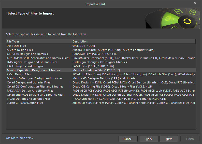
- Select Type of Files to Import—>Mentor xDxDesigner Designs and Libraries
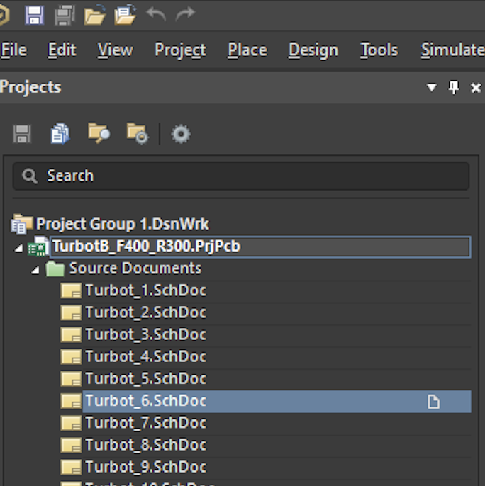
- Add the file(s) to be translated. In our example below, the “TurbotB_F400_R300.prj” has been used.
NOTE:
You can add as many .prj files at this point. However, if you add files of a different file name,
separate projects will be created.
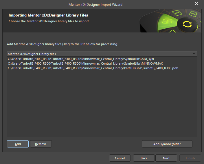
- In the next step you can add your Schematic or PCB Libraries to import (if available).
NOTE:
Because the library part and decal information is included in the source files, it is not necessary to
add libraries for schematic or PCB files to successfully translate. Only add libraries to this screen if
you wish to independently translate entire libraries for later use in Altium Designer Develop.
- Set the options for what level of reporting is done after the translation has completed.
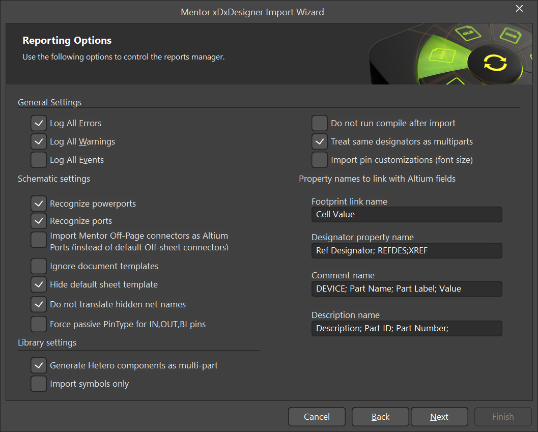
- A preview of the files being translated, and their output directories are shown. Here you can change the main output directory if desired.
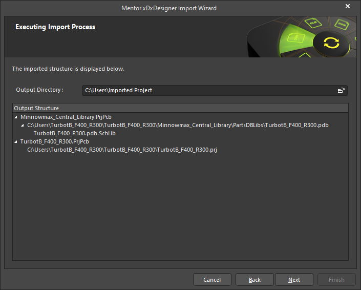
- Click the final Next button and the Import Wizard will take care of the rest.
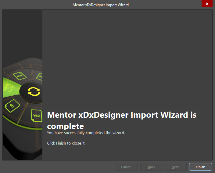
Congratulations, your schematic design has now been imported into Altium Designer Develop!
Follow the Post Import Tidy Up checks to ensure the design has been fully checked and verified. Refer to the section ‘Post Import Considerations’ at the bottom of the page.
Schematic Design File Translation
xDxDesigner project paths and schematic files translate as follows:
Project paths have an equivalent Altium Designer Develop PCB (*.PrjPcb) project automatically created for them. Once translated, files are grouped into that PCB project. For example, if you specified Example.PRJ as the xDxDesigner project, the Import Wizard will create
Example.PcbPrj in Altium Designer Develop.
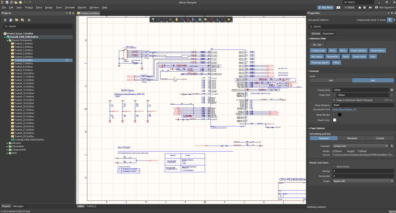
Schematic files (Name.N) translate to Altium Designer Develop schematic files (*.SchDoc). Each schematic file will be imported as a single Altium Designer Develop schematic file. Design hierarchy is maintained, including complex hierarchy.

NOTE:
Translated design files are displayed immediately after translation in the Projects panel. Once the
project has been compiled the schematic hierarchy will be shown.
Schematic Design Object Translation
Most component attributes are translated into parameters with a few exceptions:
- Power Objects - xDxDesigner symbols that contain a NETNAME attribute are identified as and translated into power objects in Altium Designer Develop.
- Ports - Similar to power objects, a symbol with an attached attribute represents it as a port. xDxDesigner symbols that contain an IN, OUT, or BI attribute are identified and translated into Input, Output, or Bidirectional ports respectively.
- Signal - Symbols that contain a SIGNAL attribute are identified and translated into hidden power pins.
- Reference Designator - The REFDES attribute attached in the xDxDesigner symbol usually has the format of: REFDES = R? When it is placed into a sheet, the user will specify the REFDES of the component in the sheet i.e., REFDES = R21.
Other common design objects translate as follows:
- xDxDesigner wire segments and busses translate to wires and busses respectively.
- A wire or bus segment in xDxDesigner can have a label attached to it. This is translated into a net label. Net label strings in xDxDesigner with the following format D [0:8] are replaced with the following format D[0..8].
- Composite symbol types are identified and translated as Altium Designer Develop sheet symbols. The symbol pin is translated as sheet entries and the sheet symbol file name will point to the list of schematic sheets that matches the symbol file prefix.
- Off sheet connectors from xDxDesigner are imported in Altium Designer Develop. Altium encourages its users to use ports rather than the Off Sheet connectors for a variety of reasons.
This documentation article provides information regarding the use of the Off Sheet connectors.
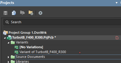
- xDxDesigner Importer supports importing project variants from xDxDesigner projects. To import xDxDesigner project variants, the following steps should be performed:
- Using the Variant Manager in xDxDesigner, export variants via Report » Delimited Text Document.
- Make sure that Unplaced is defined as the Unplaced keyword in the Settings dialog.
- Save the variant file as ProjectVariants.txt in the same location as the. prj project file to be imported in Altium Designer Develop.
- On the Importing Mentor xDxDesigner Design Files page of the Import Wizard, choose the xDxDesigner project file (.prj) – design variants will be imported automatically. The screenshot below shows Project Variants in Altium Designer Develop.
Schematic Library File Translation
xDxDesigner symbol library files translate as follows: symbol files (Name.N) translate to Altium Designer Develop library files (*.SchLib). Each symbol file will be imported into a single Altium Designer Develop library file. Once translated, files are grouped into the Altium Designer Develop PCB project (*.PrjPcb) that is automatically created.
Schematic Symbol Translation
Component Name - the following table describes how the xDxDesigner symbols translate to the Altium Designer Develop components:
| XDXDESIGNER SYMBOL | ALTIUM DESIGNER DEVELOP COMPONENT |
|
Symbol file name. For example, if the symbol file name is cap.1, the component name will be cap.1. The exception is for the hetero symbols that will be described later. |
Component name |
| REFDES attribute | Designator |
| Use from the DEVICE attribute | Comment |
| Any other symbol attribute | Parameters |
Pin Type - the following table maps the PINTYPE attribute from xDxDesigner to Altium Designer Develop:
| XDXDESIGNER PIN TYPE ATTRIBUTE VALUE | ALTIUM DESIGNER DEVELOP PIN TYPE |
| BI | IO |
| TRI | HiZ |
| ANALOG | Passive |
| OCL | Open Collector |
| OEM | Open Emitter |
Graphical Objects - Most objects have a direct translation from xDxDesigner to Altium Designer Develop. Boxes (as
defined as lower left and upper right corners) translate to four-point polygons.
Multiple-part Symbols - The PARTS attribute attached to the symbol indicates the number of parts this symbol represents and translates to the number sub-parts in Altium Designer Develop.
Annotate Symbol Type - xDxDesigner categorizes the symbol into four types: composite, pin, annotate, and module. The most common use of symbols in xDxDesigner is for sheet borders and graphical annotation. Because of this reason, such symbols are translated in Altium Designer Develop components with a TYPE = Graphical.
Heterogeneous Symbols - Heterogeneous symbols in xDxDesigner are any group of symbols that have the same HETERO attribute. When symbols are grouped under one HETERO type, they represent one device. Altium Designer Develop translates these symbols to multiple parts or display modes under one component depending on the heterogeneous type. There are three distinct types:
- HETERO TYPE 1 - Different components within the same device. The Altium Designer Develop attribute assigned to this type follows the format: HETERO = sym1, sym2, [sym3].
- HETERO TYPE 2 - Different gates within the same device. The Altium Designer Develop attribute assigned to this type follows the format: HETERO = sym, (symP) where P = PARTS number.
- HETERO TYPE 3 - This is a split IC. The Altium Designer Develop attribute assigned to this type follows the format: HETERO = (icsymname), (icsymname). The main difference between this type and HETERO TYPE 1 is only the context used by xDxDesigner related to ICs.
Translating Xpedition Files in Altium Designer Develop
- The Import Wizard can be launched from the Altium Designer Develop File menu. Choose the Mentor Expedition Designs and Libraries option as shown in the screenshot below.
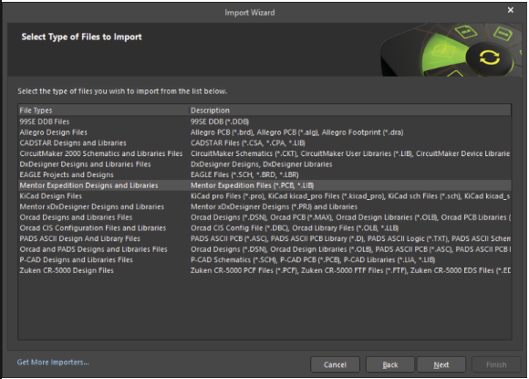
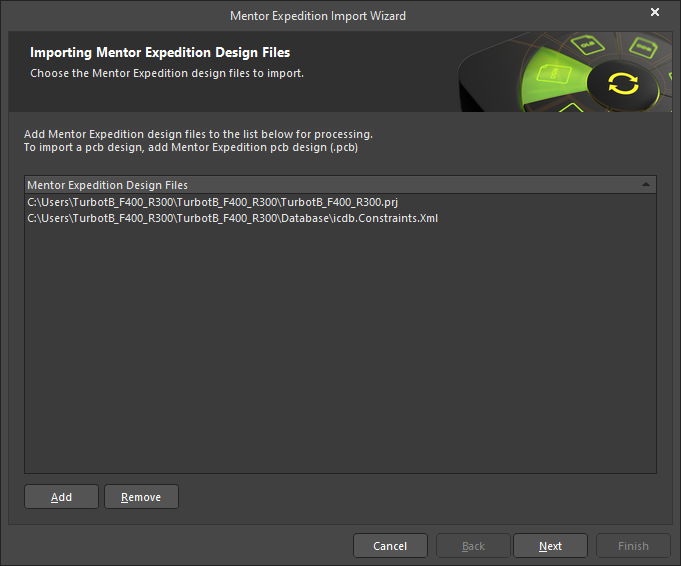
- On the “Importing Mentor Xpedition Design Files’’ screen, click the Add button to choose the (.prj) or PCB (.pcb) files. Multiple files can be translated at the same time.
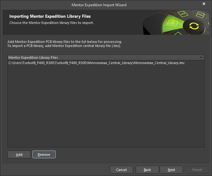
- On the ‘Importing Mentor Xpedition Library Files’ screen, click ‘Add’ and browse to the Mentor Xpedition central library file(.lmc). Step-by-step instructions on using the Import Wizard follow next.
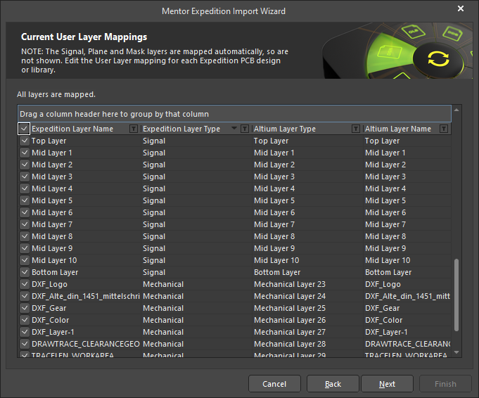
- On the screen ‘Current User Layer Mappings’. In this dialog ‘Altium Layer Type’ and ‘Altium Layer Name’ can be verified and modified as required. Clicking in these two columns allows the user to change the layer type and name using the dropdown. Layers can also be disabled during the translation.
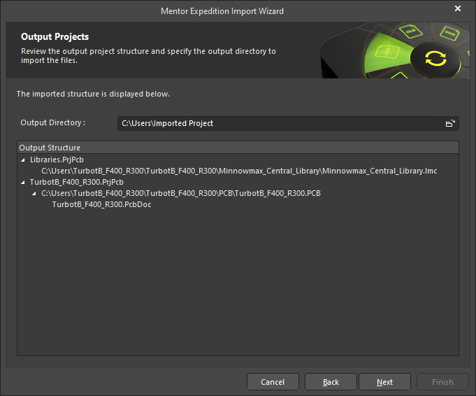
- On the ‘Output Projects’ screen, set the output directory the same as the corresponding schematic files from xDxDesigner import. This would be the best approach when the schematic and PCB both belong to the same project in the native Siemens environment. It should be noted that any folder on the user’s computer or network drive/folder can be designated as an output directory. Then click ‘Next’.
- Once the files are imported Click ‘Finish’ to close the Import Wizard dialog.
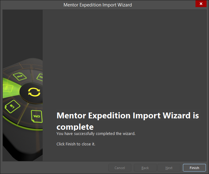
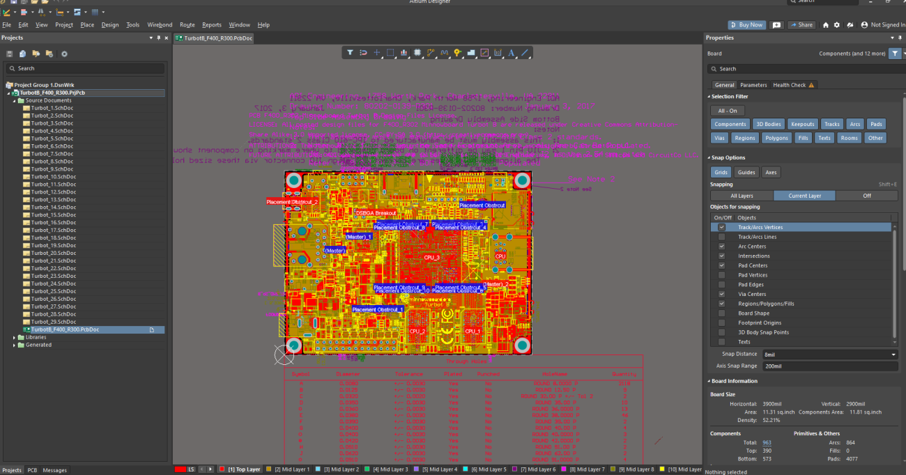
Congratulations, your PCB layout has now been imported into Altium Designer Develop!
Follow the Post Import Tidy Up checks to ensure the design has been fully checked and verified. Refer to the ‘PostImport Considerations’ section at the bottom of the page.
PCB Design File Translation
Xpedition project paths and PCB files translate as follows:
Project paths have an equivalent Altium Designer Develop PCB (*.PrjPcb) project automatically created for them. Once translated, files are grouped into that PCB project. For example, if you specified Example.PRJ as theXpedition project, the Import Wizard will create Example .PcbPrj in Altium Designer Develop.
PCB files (Name.N) translate to Altium Designer Develop PCB files (*.PcbDoc).
NOTE:
Translated design files are displayed immediately after translation in the Projects panel.
PCB Design Rule Translation
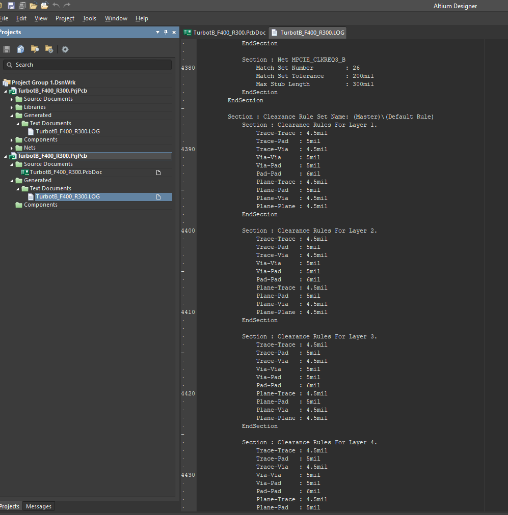
- When importing the project reference (.prj) file during Xpedition import, if there exists a a constraints file in the project directory structure, Xpedition importer automatically recognizes the (.xml) constraints file and import the constraints in Altium Designer Develop’s ‘PCB rules and Constraints Editor’. The design rules also exist in the import log file.
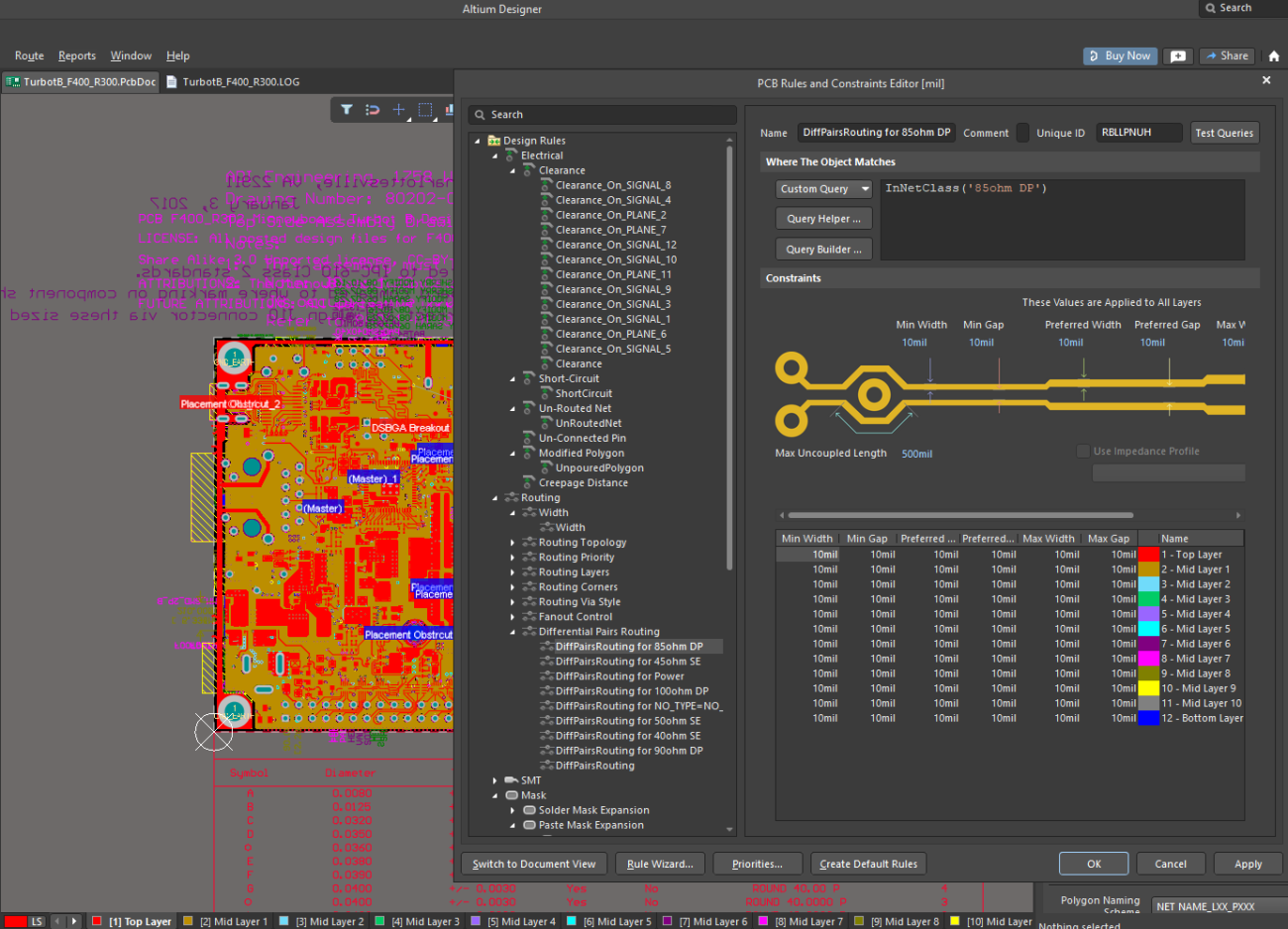
- The log file contains all the constraints imported from Xpedition software. On importing a (.pcb) these constraints can be referred from the log file and recreated in the Altium Designer Develop environment.
More details on design rules can be found in below technical documentation.
Footprint Library File Translation
Xpedition central library files consisting of decals are translated as follows: footprint files (Name.N) translate to Altium Designer Develop library files (*. PcbLib). Once translated, files are grouped into the Altium Designer Develop PCB project (*.PrjPcb) that is automatically created.
Phase 4: Post Import Tidy Up
Once your migration is complete, we recommend checking your design to ensure that all data is transferred as expected. Below is a list of key checks to perform post-migration:
Physical check
- View » Fit Document
- Board shape and cutouts
Electrical check
- Netlist
Rules
- Have all rules been imported
- DRC check
- Check settings for polygons - Island removal, min primitive size
- Thermal reliefs, direct connect
- Check power plane settings
- Power plane Pull-back
- Solder mask, Paste mask rules
- Via Tenting
- Testpoint assignments
Power check
- Nets
- Planes
- Polygons
Documentation check
- Layers
- Text/Strings
- Legends
PCB reports
- Number of components/nets
- All nets routed
Reference Tech-Doc - Post Import Consideration
Getting Help
Main article: Documentation and Help
The best way to learn is through doing, Altium and Altium Designer Develop provide a number of ways to help you do that:
- Press F1 with cursor over any object, editor, panel, menu entry, or button to open a brief description in your web browser
- Use shortcut Shift+F1 while running a command for a list of shortcuts you can use in that command.
- Altium Designer Shortcut Keys
- Search the Altium Documentation, on the Altium website
- Visit the Video Library where you can watch over 150 short training videos, each detailing the exact steps needed to complete a task.
Image illustrating pressing Shift+F1 during active interactive routing command
See Also
Below are references to other articles and tutorials in the Altium Designer Develop Documentation Library that talk more about the conceptual information as well as walk you through specific tasks. Remember, you can also browse through the Help contents, and use F1 and What’s This at any time in a dialog for more details.
- For more PCB project options, refer to the tutorial, A Complete Design Walkthrough with Altium Designer Develop
- For a tutorial that steps you through all the basics of creating components, read A Look at Creating Library Components.
- For a tutorial that steps you through all the basics of editing multiple objects, read Editing Multiple Objects.
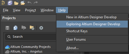
On the top left of Altium Designer Develop you can also find the Help » Exploring Altium Designer Develop.
From here, you can easily access the Documentation where the “Getting Familiar with the Altium Design Environment” category will ease your beginning into using Altium.
Contact
Website: www.altium.com
Head Office: Address: 4225 Executive Square, Suite 800, La Jolla, CA 92037
Phone: +1 858-864-1500
Related Technical Documentation
Table of Contents
Design to Release, Without the Friction
- Keep reviews tied to the right version
- Reduce handoff confusion and rework
- Spot sourcing and release risk earlier
- Work solo, share when needed
Get Started
Thank you, you are now subscribed to updates.

