


Best Practices: Snapping Usage in the PCB Editor


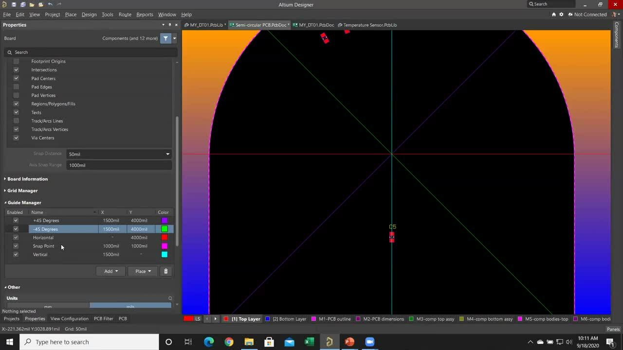
Getting your PCB layout design done takes patience and precision. Complex footprint geometries, board shape, and dense component placement require accurate primitive positioning. Each stage of PCB design needs a different snapping configuration. Often your settings can be excellent fit for one stage and be unfavorable for another. For example, good snapping settings for your board outline can make routing almost impossible. Learn more about different snapping usage patterns and best practices of efficient snappings.
Related Resources
Related Technical Documentation
Design to Release, Without the Friction
- Keep reviews tied to the right version
- Reduce handoff confusion and rework
- Spot sourcing and release risk earlier
- Work solo, share when needed
Get Started
Thank you, you are now subscribed to updates.