


Defining High Speed Signal Paths in modern PCB Design


This on-demand virtual session covers basic and advanced design challenges that designers and PCB engineers face. It provides instruction with value and insight on the typical design and layout related topics ranging from simple to technically complex solutions incorporating best practices.
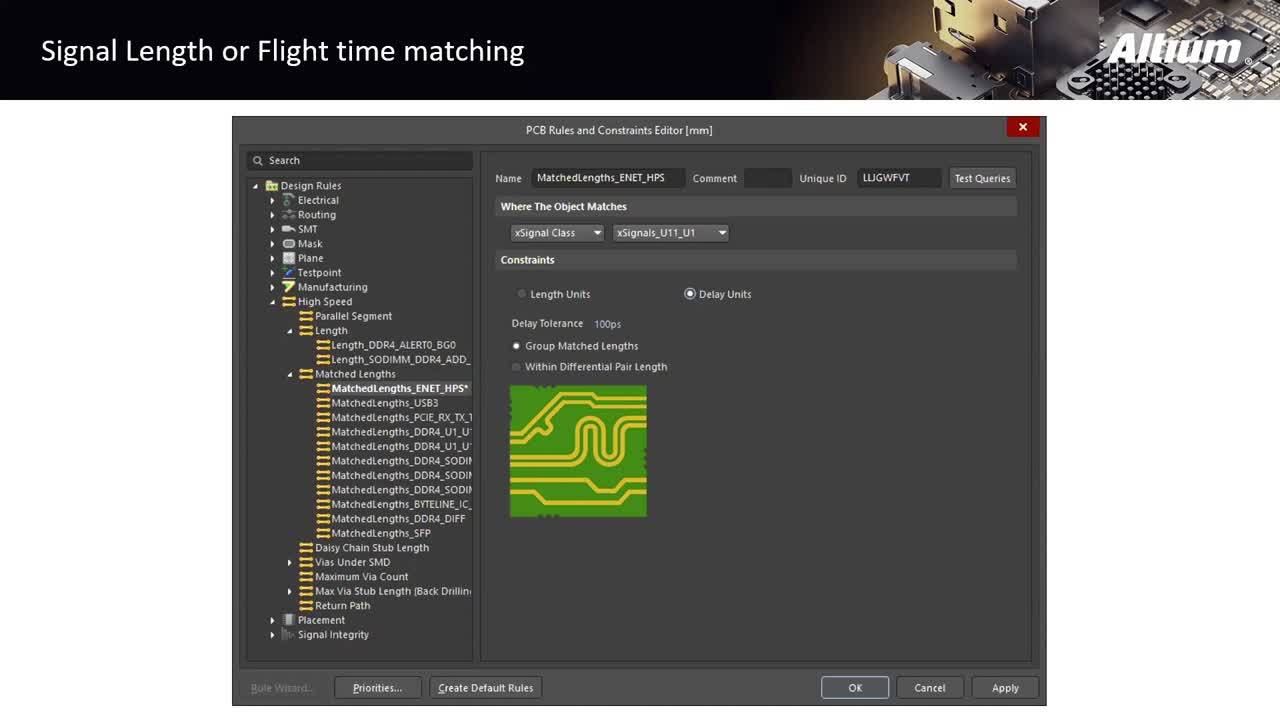
This track provides insight about how challenges regarding switching speeds in modern high speed devices can be addressed and converted into a solid and robust PCB Design using up-to-date tools and methods. Learn how to effectively set up Layer stackups, Impedance Control and Return Paths, and properly tune signal lengths and flight time.
Related Resources
Related Technical Documentation
Design to Release, Without the Friction
- Keep reviews tied to the right version
- Reduce handoff confusion and rework
- Spot sourcing and release risk earlier
- Work solo, share when needed
Get Started
Thank you, you are now subscribed to updates.