Flyback Converter Module PCB Design Project

If you have an electronic product that converts AC to a moderate voltage DC while also providing isolation, then most likely you're using a flyback converter. Flyback DC/DC converters give the large step-downs required in AC-connected systems that also require a DC output, but without a big hit to efficiency. In this project example, I'll show how to design a basic flyback converter module, both in schematics and in a PCB layout.
Flyback converters require a transformer, and the transformer you use will determine the level of step-down and current handling that the device can handle. A big part of flyback converter design is the transformer design and selection, which could force you to use a custom transformer. We'll see how this arises in this project. At the end of this article, you'll have a chance to download the design files and start using them in your own designs.
Getting Started With a Flyback Converter
The flyback converter design I will show in this project is meant to convert 120 V AC input down to a 3.3 V output. The primary controller that will be used to run the flyback converter is the UCC28881 from Texas Instruments.
At a basic level, the device we want to design includes three stages:
- AC input, circuit protection, and rectification
- Flyback converter switcher and transformer
- Output interface and isolated feedback loop
The schematics shown below illustrates each of these three stages connected together to produce the 3V3 output. This system is expected to handle 1-2 A of current. This system is also going to maintain isolation provided by the transformer, which requires careful placement of all of the components.
AC Input
The input leading to our transformer contains circuit protection components and a bridge rectifier (BR1). The circuit protection provided here includes a fusible resistor, metal oxide varistor, and a small amount of capacitance. On the output side of the bridge rectifier, we have a TVS diode and some additional capacitance to reduce ripple from rectification.

The goal of this section is to rectify the input AC and provide a semi-stable DC output to the switcher section while also providing circuit protection. Here, I have not added EMI filtering, but this could be added with low-pass filtering and some chokes (see below). How you add those elements depends on whether you will keep the chassis connection after the AC input. For now, let's proceed with a line and neutral connection and omit the earth connection.
Switcher Circuit (UCC28881)
The switcher circuit is based on part number UCC28881, which is an open-drain switching controller that includes a feedback connection and supports a wide input voltage range. The snubber circuit (made up of C1, R1, D1) provides stability during switching so that large overshoot/undershoot during switching can be suppressed.

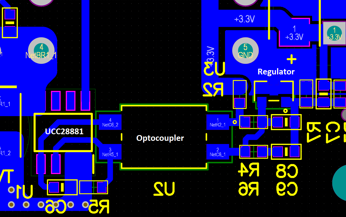
3V3 Output and Feedback
The output stage is shown in the image below. This shows how the output is rectified down to a DC output via D2 and finally stabilized with some capacitors. The output section includes some testpoints for manual probing if desired, as well as a terminal block to attach flying leads. Note that C8 is marked DNP and is optional; its placement can provide further stabilization if required and can easily be determined from a comparative measurement with a scope.

The feedback section uses an optocoupler and a precision shunt regulator to stabilize the power through the optocoupler. The resistor divider R3/R7 biases the REF pin on the LMV431AIMF regulator to 1.244 V. The additional passives provide filtering/stability when the system is biased ON and the LMV431AIMF also switches from OFF to ON. The R2/R4 voltage divider biases the optocoupler to the correct voltage and current, and it will only allow current flow when LMV431AIMF is biased ON.
Transformer Design and Selection
Flyback converters use a transformer and its primary side inductance in order to step up/down the input voltage and regulate the output voltage. They are switching regulators that use the primary side inductance as a typical buck converter would use a regular inductor.
To properly size the transformer, we need to determine the required duty cycle, coil inductances, and peak currents. First, we need to determine the turns ratio for T1, which depends on the desired output voltage (Vout) and the diode forward voltage drop (Vdiode, measured on D2 above). This will also determine the duty cycle for the switcher:
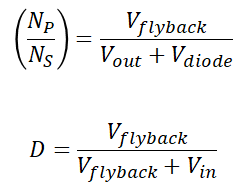
If you have an off-the-shelf transformer that has a specified turns ratio, then the flyback voltage can be determined. Or, if you want your switcher to run at a specific duty cycle, then you can determine the flyback voltage and thus the required turns ratio.
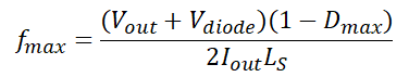
Next, we can determine the required maximum switching given the maximum duty cycle capability and the target output current.
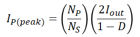
Next, to help size the transformer, there is a requirement on the peak current:
The challenge with designing the transformer for a flyback converter is finding a transformer that balances the form factor, inductance value, turns ratio, and current handling limit. Most transformers that you buy off-the-shelf will only hit 2 or 3 of these requirements. From what I have seen, most of these off-the-shelf transformers that offer the required turns ratio and current handling, but they won’t give the required form factor.
This means you may need to design a custom transformer or work with an assembler to build a custom transformer. There are core and bobbin components available that can be used to assemble a custom transformer that will hit your inductance and turns ratio specs in a specific form factor. You will need to carefully assemble a custom transformer or contract with a vendor to have the component assembled.

The design shown below will use a TDK core insert (PN: B66417G0000X149) and TDK coil former (PN: B66418W1008D001), which is a through-hole part that could allow for center tapping if desired. Based on the target output voltage of 3.3 V and a reasonable switching frequency of 62 kHz for the UCC28881, the required turns ratio is 69:4 and the primary inductance is 984 uH. The peak current handling does not need to be excessively large for a low-power flyback converter module, which allows a small wire diameter of 26 AWG for the windings. The expected peak primary current is 0.44 A.
PCB Layout
The PCB layout is shown in this section and it is relatively simple to understand the approach to this layout. The goal here is to illustrate how to maintain the isolation required for this DC/DC converter and how to implement this in a module form factor.
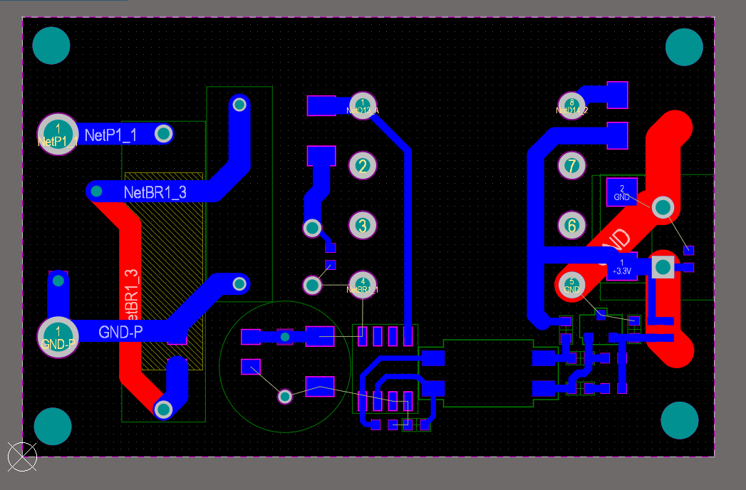
The initial placement is shown below, and the isolation boundary is marked using the dashed white line. All of the large through-hole components have been placed on the top layer, while the smaller SMD components have been placed on the bottom layer. The AC input will attach using flying leads that solder to plated holes (left side), and the 3.3 V output is taken from a 2-screw terminal block (right side).
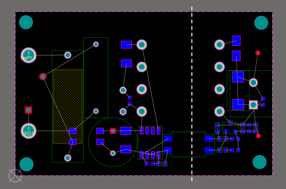
The IC that is spanning across the isolation barrier is the optocoupler (U2). This feeds directly into the UCC28881 switcher (U1) and completes the feedback loop. The placement of the optocoupler is such that it ensures a consistent isolation gap near the middle of the PCB.
To start routing, I first set some clearances that ensure sufficiently large spacing between parts in the design according to the IPC-2221 standards. You can calculate these required clearances using the data shown in this article. The clearances I use assume a 120 V AC input on the primary side.
Next, the routing is completed with somewhat large traces to ensure sufficient current handling on the primary and secondary sides. Note that there is a decently large gap around the power input traces (line and neutral), which could be a region where noise is received/emitted. It may be desirable to use larger polygons as pours to limit noise generation and reception at low frequencies.
Now we can draw in the remaining polygons to provide ground for the output and the switcher. These are drawn out below. I have also cleaned up the silkscreen to prevent clearance errors and overlapping designators. The large sections of copper shown below both provide ground for the switcher to help ensure shielding, and it will provide current handling capability for BR1.
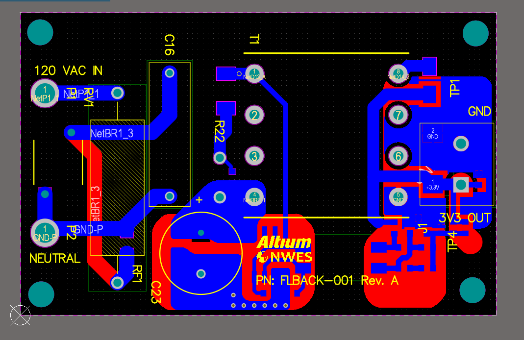
This completes all the routing and cleanup required for the design. The transformer is a switching element that could be rather noisy, and addressing this is one of the potential changes that could be implemented in the design.
Ideas For Expanding This Design
At its most basic level, this circuit will be functional and show high efficiency. It has all the basic elements needed for the design to function as an AC-to-DC regulator module. Of course, I always like to do a short section on how the design could be improved or expanded. The ideas I list below are not requirements for functionality, although they can help make the design better from an EMC perspective or reliability perspective.
- Add a Y-type capacitor across GND-P and GND
- Place chokes on the input and output side if common mode noise is a problem
- Add a cutout between the transformer and optocoupler leads to clearly denote the isolation region
- Add an additional secondary tap and change the winding ratio to produce a dual rail module
- If placed in a metalized enclosure, add a chassis guard ring and connection to earth
- Remove the input solder holes and add a standard receptacle for an AC plug
To improve the design for EMI/EMC, the first two points in that list are important. Regarding the first point, this is a typical way to bridge grounds in an isolated DC power supply as it helps control return paths for high frequency signal components originating from the switching waveform. If there is a problem with high frequency radiation from the 3V3 side, then this can help suppress that.
The second point is important in general for EMC. Creating a front-end EMI filter using an LC filter (pi filter) and placing chokes on the input will suppress common-mode radiation coming from the AC line input. The output will connect to wires or a cable as well, and we would like to eliminate common-mode radiation on that cable, which may also require a common mode choke.
To download the original project files, follow this link. These files are available under a CC license.
Whenever you want to build stable and reliable power systems, use the complete set of PCB design features and world-class CAD tools in Altium Designer®. To implement collaboration in today’s cross-disciplinary environment, innovative companies are using the Altium 365™ platform to easily share design data and put projects into manufacturing.
We have only scratched the surface of what’s possible with Altium Designer on Altium 365. Start your free trial of Altium Designer + Altium 365 today.

About Author
Related Resources


Related Technical Documentation


Table of Contents
Take advantage of the world's
most trusted PCB design system.
One interface. One data
model. Endless possibilities.
Effortlessly collaborate with
mechanical designers.
The world's most trusted
PCB design platform
Best in class interactive
routing
View License Options
Thank you, you are now subscribed to updates.