The Breadth and Depth of Your PCB Design Workflow
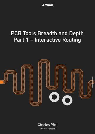
The routing process remains the most time-consuming layout task, Altium Designer interactive routing technology makes design dense board layouts much easier.
Modern printed circuit boards must address a broad set of technology challenges. PCB design software needs to include tools that help design engineers stay productive while ensuring new designs are fully manufacturable. Designers that create advanced technology rely on interactive routing tools in their PCB design workflow to remain productive and create advanced designs. If you’re looking for the best interactive routing features, you need to use the comprehensive suite of design tools in Altium Designer, the industry’s only fully integrated PCB design software platform.
ALTIUM DESIGNER
A professional PCB design platform with a complete set of design tools in a single application.
For most designs, routing is the most time-consuming task in the PCB layout process. As technology in PCBs has evolved over many years, routing software has advanced to support those requirements. The Altium Designer interactive board layout routing environment provides support for any topology, as well as HDI/BGA breakout, flex, and rigid-flex designs.
Altium Designer does more than just provide support for standard routing requirements. The routing features in Altium Designer are interactive, making it easy to quickly route multiple traces in your design as you create your PCB. You can go a step further and check signal integrity in your high speed PCB, and all without using an external simulator. The interactive routing features in Altium Designer help you create a productive PCB design workflow.
From Autorouters to Interactive Routing
Over the years, many tools have been developed to help you stay productive during design and layout. Autorouters are one of the most well-known tools for automatically placing traces between components. However, these features often require cleanup and can create more work than they eliminate if not used correctly.
For this reason, auto-interactive routing features (or simply interactive routing) were developed to give designers more control over their routing results. These tools apply the same set of design constraints to groups of nets, and the designer can set waypoints for traces between sources and loads. The interactive routing engine fills in the gaps, leaving less cleanup once routing is completed.
Stay Productive with Interactive Routing
The best-in-class routing tools use interactive routing to quickly route groups of traces around your printed circuit board. Interactive routing helps you stay productive by applying the same routing pathways and rules to groups of nets, such you would normally use in high speed digital interfaces. Compared to autorouters, your interactive tools give you more control over the results with less cleanup.
- Interactive routing is a major advance over autorouting as it gives designer control over an automated process.
Learn more about the difference between autorouting and interactive routing.
- Not all interactive routing features are created equal, and some design platforms don’t contain much beyond a simple autorouter. Altium Designer’s interactive routing features give you control over the routing process for advanced designs.
Learn some helpful tips for interactive routing in Altium Designer.
- Your interactive routing features shouldn’t limit you to a single-ended topology. You need routing features that accommodate advanced high speed interfaces, such as DDR3/DDR4.
Learn more about using interactive routing for fly-by routing topology in DDR3/DDR4.

Routing a dense PCB in Altium Designer.
Interactive Routing and Layout for High Speed PCB Design
Creating complex high speed designs requires plenty of time routing and laying out components. Your routing tools need to have built-in features that apply important routing structures to ensure signal integrity. Common interfaces like DDR3/4 and USB3.0 signals need controlled impedance traces with differential pair routing to ensure low noise high speed communication.
The routing tools in Altium Designer do more than just let you quickly route multiple traces. The semi-automated routing tools in Altium Designer check your signal behavior against high speed design rules with an integrated field solver. There are other important tasks required to satisfy specific design rules for differential pairs and controlled impedance signals, and you’ll find everything you need for high speed design in Altium Designer.
Ensure Signal Integrity with Interactive Routing Features in Altium Designer
The xSignals package delivers fully configurable single-ended and differential pair routing with length tuning, as well as important numerical calculations for signal integrity. Impedance mismatches, overshoot/undershoot, crosstalk, and impedance mismatches can be quantified from your PCB layout for selected groups of nets. When you need to ensure length matching in parallel nets, the interactive routing tools in Altium Designer allow you to apply standard length tuning structures to maintain propagation delay and differential impedance.
The core challenges in high-speed design center around controlling impedance and ensuring you length matching in critical nets. Altium Designer’s interactive routing and CAD tools interface directly with your design rules to give you full control over these features, providing dynamic means to optimize and control net and differential pair lengths. This is implemented by allowing variable amplitude wave patterns to be inserted according to the available space, rules, and obstacles in your design. With intuitive control, the length tuning properties can be based on design rules, properties of the net, or values you specify.
- Altium Designer supports multiple length tuning features, which you can mix and match in an interconnect.
Learn more about standard length tuning structures for high speed signals.
- Differential pairs need precise length matching to ensure common-mode noise suppression, as well as consistent impedance and propagation delay.
Learn more about differential pair length and phase matching.
- Other effects like pin-package delay need to be added to your propagation delay to ensure length tuning and consistent impedance during routing. Altium Designer allows you to set pin-package delay values in your component models.

Differential pair length tuning structures can be quickly placed in your PCB layout in Altium Designer.
Use the Interactive Routing Features in Altium Designer
Altium Designer is the only circuit board design software that gives you everything needed to design the highest quality PCB layouts in a fraction of the time. The advanced routing engine includes push and shove, hug, walk around, and interactive length tuning modes for single and differential pair routes. This is all available in a single program alongside the other important design features you need for routing and layout in a single program.
An Integrated PCB Design Workflow
The strength of Altium Designer comes from its underlying rules-driven design engine. This allows the routing features shown here to be integrated into a single program along with your other important design features. You can create hierarchical multi-channel schematics, intricate PCB layouts, and a complete set of manufacturing documents in a single program when you use Altium Designer.
The rules-driven design engine interfaces with all your design features, meaning your layout is checked against your design rules as you create it. Other design platforms force you to complete a layout, then run batch DRCs to locate routing and layout rules violations. Instead, you can catch and correct errors early when you make Altium Designer the backbone of your PCB design workflow.
- Take your design from simple circuit diagrams to full-scale manufacturing when you use the design features in Altium Designer.
Learn more about the integrated set of PCB design tools in Altium Designer.
- Layout and routing go hand-in-hand, and the powerful CAD tools in Altium Designer let you implement industry-standard routing features in your PCB layout. Take full control over your routing with the design tools in Altium Designer.
Learn more about the powerful routing features in Altium Designer.
- The process to migrate from Cadence to Altium Designer is simple. You can reuse your old projects in the world’s only unified printed circuit design environment.
Learn more about layout and routing for rigid-flex PCBs in Altium Designer.

ActiveRoute with length tuning in Altium Designer - before and after - 25 seconds later!
Your productivity shouldn’t be hampered by outdated design tools that make routing difficult. Try working in Altium Designer’s unified environment for PCB design. You’ll have access to the most advanced routing features to speed up your layout and signal integrity processes.
Altium Designer on Altium 365 delivers an unprecedented amount of integration to the electronics industry until now relegated to the world of software development, allowing designers to work from home and reach unprecedented levels of efficiency.
We have only scratched the surface of what is possible to do with Altium Designer on Altium 365. You can check the product page for a more in-depth feature description or one of the On-Demand Webinars.
 Open as PDF




 Back
Back