


Differential Pair Length Matching: Best Practices for Signal Integrity

At a Glance
Length tuning/delay tuning is one important aspect of high speed routing with differential pairs. Read on to learn all about Altium's differential pair length tuning capabilities.


Conceptually, differential pairs are very simple, being just a pair of equal and opposite polarity signals running on two parallel conductors. In terms of signal integrity, differential pair routing becomes progressively more difficult when frequencies get higher. At the low end of the possible range of rise time values and frequencies, timing is the main constraint, while at faster rates we see issues with skew, mode conversion, and bandwidth limiting due to losses.
To ensure timing within some required margin, lengthening structures are applied along the length of the differential pair route. You may also have length tuning applied between multiple differential pairs and a parallel interface, such as CSI or specialty logic instantiated over LVDS. Of course, there are important requirements for successful link tuning, and the use of length tuning has an impact on signal integrity, which is normally not considered until channel qualification.
To help ensure you reach success with linking structures, I'll provide some simple guidelines that can help you eliminate signal integrity problems from length tuning structures in your PCB and to determine the optimal amount of length tuning needed in a differential pair, as well as between multiple differential pairs. Judicious use of length tuning balances precise timing against a new SI/EMI problem known as mode conversion, especially when designing for multi-Gbps interfaces.
Two Types of Differential Pair Length Tuning
Differential pairs require two types of length tuning to ensure a differential receiver can recover a logic state from an incoming bit stream:
- Intra-pair length tuning: The two trace lengths in a differential pair are adjusted so that the signals making up the navigating differential signals are lined up in time. This length tuning relies on the rise time of the differential signal.
- Inter-pair length tuning: Length matching is enforced between multiple differential pairs so that multiple differential signals are lined up in time. This length matching is typically based on some fraction of the UI time.
Serial buses require the length tuning between the two traces only; they do not require inter-pair length tuning because there is only a single differential pair, or because multiple differential pairs have no required timing relation. This is where you get the type of trace routing with serpentine routing sections as shown below. In this example, there are 6 differential pairs being routed as striplines; the bends in the breakout region create some skew, but once the pairs complete breakout there is enough room to apply the length tuning regions. These are small sections that have been placed reasonably close to the breakout region.
Parallel buses, which typically have a source-synchronous differential clock, require both types of length tuning. Common examples include parallel LVDS, MIPI interfaces, PCIe, and gigabit or faster Ethernet.

Single Differential Pair: The Rise Time Window
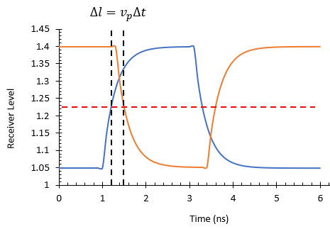
All length tuning structures are implemented not just to equalize the length of the traces within a single differential pair. Really, it is to provide delay such that the opposite polarity signals on each end of a differential pair are aligned in time. Differential receivers are crossing detectors, so the timing requirement is that the two signals must be switching at the receiver at the same time. This gives us a timing window, which is a bit less than the rise time, and the signals must arrive at the receiver within the required time window in order to switch simultaneously and thus define an incoming logic state.
Using the differential signal velocity on the PCB layer carrying the routing to the differential receiver, the timing window can be converted to a length mismatch tolerance as shown in the graph below.
Now, whenever you set up a length mismatch or timing mismatch constraint in your PCB layout, the PCB editor would use the physical length you have set down for the traces in your PCB to determine a length mismatch. If the propagation delay for the signals on the interconnect is known, then the corresponding timing mismatch can also be determined by the PCB editor. This is then checked against the length constraint in real time as you apply the length tuning structure. Advanced PCB design software, including Altium, allows users to define the mismatch as either a length or a time delay; note that if a time delay is used that the signal propagation velocity must be defined somewhere in the PCB editor.
How Close Should You Tune Trace Lengths in a Differential Pair?
There is no specific value required for differential pair length tuning. Technically, any remaining timing mismatch that is less than the timing window (as illustrated in the above graph) can ensure the interface is fully functional as long as there is no additional jitter seen at the receiver (see below for details on this).
This leaves a lot of room for your differential pair length tuning margin. For example, let us suppose that we have a timing window of 100 ps; if we have loosely spaced traces in a differential pair routed as striplines on the Dk = 4 substrate, then the allowed length match will be:
ΔL = (1.5e11 mm/s)*(100 ps)*(39.37 mil/mm) = 591 mil
Obviously, this is a very generous amount of length mismatch, and you would be able to accommodate this mismatch easily in any CAD system.
Some component datasheets will state a fixed value for maximum allowed length mismatch and will not mention a timing mismatch at all. If you ever see a nice round number for allowed length mismatch, such as 100 mils, it is probably an arbitrary value, or it will be a very conservative value but still an estimate (the real mismatch allowance is proabably larger). Furthermore, as we saw in the above calculation, the link mismatch depends on the dielectric constant of the substrate material, i.e., the signal propagation velocity, but the datasheet may never mention a qualifying dielectric constant for their specification.
The Actual Timing Window is an Allowance For Jitter
While the math tells us that a 100 ps timing mismatch will still allow a differential interface to function, should we actually include 591 mil of mismatch as the example tells us? The answer is of course no. The reason is that this timing margin needs to account for all possible sources of timing error, or in other words, the total jitter that can be expected in a differential channel.
In my high-speed design seminars, I often refer to a quote from Steve Corrigan of Texas Instruments, who nicely stated a definition of jitter:
- Jitter is the sum of all skews
What Steve was referring to was jitter being the sum of all deterministic and random sources of timing mismatch. There are many sources of random, fluctuating skew (what we most often refer to as jitter) and deterministic skew:
- Crosstalk from nearby transmission lines
- Reflections at the receiver or at impedance mismatches
- Transient ringing on the PDN, a.k.a. power system noise (PDN ripple and ground bounce)
- Noise from fiber weave, including in laminates with spread glass
- Mode conversion (more on this below)
Something very important should be understood about the above items:
- None of these sources of skew occur simply because there is a length mismatch within a differential pair. These skews will always be present. Reducing the length mismatch to zero does not eliminate these sources of jitter.
When length tuning is applied, we need to get the timing mismatch small enough that there is plenty of margin to account for all of these other sources of skew. This will ensure that trace-to-trace skew is within spec for your interface standard, and the intent is to ensure the signal remains as a differential signal within the required channel bandwidth throughout the length of a route (minimum mode conversion).
If the signal experiences appreciable jitter, the interface can still work as long as the jitter occurs within the timing window; the same applies to skew from the fiber weave. This can occur even when the trace lengths are perfectly matched; this is why it’s best to match lengths/delays as close as possible in your CAD tool: there will always be a little bit of jitter and you need to leave margin for it in the timing window.
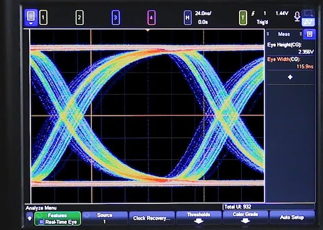
Jitter can be measured directly in an eye diagram or determined from a simulation, such as the oscilloscope readout shown below.
Once we account for total jitter seen at the receive side of the differential pair, actual allowed timing mismatch will be less than the rise time; in our above example calculation with a 100 ps rise time, jitter could reduce the allowed mismatch significantly.
Rules for Applying Differential Pair Length Tuning
These very high-level guidelines apply to both If you route a differential pair and you find that you do need to apply link tuning to the route, there are three very simple rules that help prevent ensure signal integrity:
- Start by designing the pair with loose coupling and preference for a thinner PCB laminate
- Keep length tuning structures as short as possible
- Apply the length tuning exactly where skew arises
- Try to get the length mismatch as small as possible, but it does not need to be exactly zero
- If routing on multiple layers, apply the length tuning on each layer individually
Principally there are two signal integrity problems these guidelines address: these are mode conversion and reflection at the input of the length tuning structure.
Problem #1 in Length Tuning: Reflections
Unfortunately, you do not have the freedom to apply infinite amounts of length tuning. As I mentioned above and show in the linked article, all length-tuning structures create some mode conversion and there will be an impedance mismatch as the differential signal encounters the length tuning section. There will be some reflection off of the length tuning structure as the signal approaches it. The frequency range where this is noticeable depends on the size of the length tuning structure, i.e., the amount of skew that you are trying to compensate.
To see an example of just how much impedance mismatch and mode conversion a length tuning structure might create, take a look at the S-parameters below. These S-parameters and TDR plot below were computed for a 90 Ohm differential pair with a small amount of length tuning applied due to a 50 mil mismatch; these were simulated using Simbeor. Without the tuning section, the return loss shows -40 to -30 dB.


If, instead of having one long tuning structure, we broke it up into smaller tuning structures at specific locations where the delay arises, the reflections and mode conversion would be pushed out to higher frequencies.
This is why there is often a guideline about differential pairs and high-speed signals in general, which states that the signals should be as straight and direct as possible; it is to avoid applying length tuning or at least minimize its use. This is necessary because, on multi-Gbps interfaces, there are allowed mode conversion limits that must be obeyed in order to ensure the differential channel is compliant with the interface standard.
Problem #2 in Length Tuning: Mode Conversion
Length tuning structures help align signals in time by enforcing a delay, but they represent an inherent differential impedance discontinuity along the length of the route. In particular, the length tuning structure will have its own input impedance, which will be a function of frequency and the length of the tuning structure.
Suppose you have a long route and you need to apply a large amount of length tuning to restore signal edge rate timing along the differential pair. Where should small sections of length tuning be placed? The answer is in rule #3, such as in the example shown below. These small sections of length tuning structure are applied right at trace bends and are only made as long as is absolutely necessary. One of these sections can be placed at each bend along this route.
- We prefer to follow rules #2 and #3 because it will push strong mode conversion out to higher frequencies
The image below shows the mode conversion we could expect as a function of frequency due to application of the length tuning section shown in the return loss/TDR plots above. The curves in this plot show the conversion between differential signal and common mode signal, essentially telling the designer how much additional loss will occur in the channel above the standard (conversion-less) insertion loss. This occurs because the channel converts some signal into common mode, and the differential receiver then destroys that common mode with very high suppression ratio.

Do you always need to make differential pair length tuning structures extremely short? It all depends on the required channel bandwidth. Mode conversion created by length tuning structures is a bandwidth limiting effect, and so your channel design should account for this based on the bandwidth required at the receiver.
Because this is all based on input impedance, the differential pair length tuning structure will have the following properties:
- Longer length tuning structures will exhibit more mode conversion at lower frequencies
- Larger amplitude in the tuning structure may create more mode conversion
Following design of the differential route, the channel should be simulated to verify channel bandwidth and mode conversion.
Timing Example For a Single Differential Pair
Suppose we have a 500 Mbps differential interface where the typical signal rise time is 100 ps on the PCB given in the example above, equating to 591 mil of allowed mismatch.
Suppose also that the expected skew along the length of the route is 10 ps per inch; a two-inch route would give 20 ps of skew from the PCB. Let's also suppose that SI simulations show that reflection from the receiver, ground bounce, and crosstalk produce another 35 ps of skew shown in an eye diagram simulation.
In this case, the actual length tuning tolerance is not 591 mils because the skew allowance is only 45 ps, not 100 ps. Therefore, the length mismatch allowance is:
(45 ps/100 ps) * 591 mil = 266 mil
Length Tuning Conditions for Multiple Differential Pairs
When multiple differential pairs are part of the same interface, the length tuning condition is typically no longer represented as a rise time. The reason for this is that there is often a source-synchronous clock which defines the timing conditions for the bus. In these cases, the jitter tolerance can be a fraction of the UI value for the interface's data rate. The UI interval can be converted to a timing mismatch, and then to a length mismatch.
As an example, let's suppose the above 500 Mbps interface is actually a 500 Mbps per lane interface with four differential pairs. If the maximum timing mismatch allowance across the bus is 0.15 UI, then the timing mismatch is:
1 / (500 MHz) = 2 ns
0.15 * 2 ns = 300 ps
As we can see, parallel differential interface timing mismatch allowances expressed as a fraction of UI can be quite long. Once again, the question arises, should we actually use this 300 ps limit for length tuning?
Again, the answer is no, because we have to allow for all other sources of skew to contribute to the timing jitter seen within this window. In parallel differential buses that are not too close together on the PCB, the most significant source of timing jitter is inter-symbol interference (ISI), also sometimes referred to as data-dependent jitter. This primarily arises due to reflections off the input buffer on the receiver component at high frequencies, so each bit impacts the timing of all subsequent bits. When the bus is dense and differential pairs are close together, differential crosstalk also contributes to the timing jitter observed between the lanes in the differential bus, and it will also contribute to the ISI observed in an eye diagram.
Of course, skew in the PCB, cable connections, connectors, and random/pseudo-random sources of skew all contribute to the total jitter observed in these interfaces. There are also test standards for qualifying whether an interconnect design is compliant with the interface specification, which will attempt to quantify skew at each of these elements in the interconnect.
Differential Pair Tuning in Altium Designer
When you need to apply length tuning sections based on either timing mismatch or length mismatch, your PCB design software can help construct the tuning section and check against the timing constraint.
Example With 90 Ohms Differential Pairs For USB
Once you’ve created your schematic and decided on a layer stack, you’ll need to create an impedance profile. If you open the Layer Stack Manager in the PCB Editor window, you can go to the Impedance tab to create a new impedance profile. Here, we want to create a differential-pair impedance profile set to 90 Ohms differential impedance with 15% tolerance. To do this, keep the Impedance tab open and bring up the Properties panel. You can define all aspects of the differential pair (including copper roughness) in your manufacturing process, directly in the Properties panel.

Defining a differential pair impedance profile in Altium Designer
Setting Design Rules
Once your differential impedance profile is defined, you’ll need to bring it into your design rules.Once your differential impedance profile is defined, you’ll need to bring it into your design rules. We need to modify the default design rules so that the differential impedance profile we defined above applies to the differential pair routing tools. To do this, click the “Design” menu, then click on “Rules…” This will bring up the PCB Rules and Constraints Editor, as shown below. Here, we want to create a new rule that applies to the differential pairs to be routed between the USB PHY interfaces and the USB hub component.
Here, you need to create a new rule and select the nets to which it will apply. You can also set this new rule to apply to an entire layer if you like. Once you create the new rule, check the “Use Impedance Profile” box and select the differential impedance profile you defined (mine is “D90”).

Selecting a differential pair impedance profile for your USB nets
Finally, you can set your length matching tolerance or your delay tuning tolerance in the design rules dialog. Under the High Speed design rules section, you can set the delay/length tolerance in the Matched Lengths section. This can be set to apply only specific differential pairs, or to all differential pairs. If you need to apply length matching for multiple differential pairs, you can create a rule that takes top priority and applies to Group Matched Lengths.

Defining length targets for a differential pair
Length Tuning
After you’ve routed your traces, you’re ready to match trace lengths. To get started, you can match individual traces within a differential pair to ensure the two ends meet the length tolerance requirements. This is done using the single-ended Interactive Length Tuning tool in the PCB Editor, as you want to adjust individual traces to the correct length. Clicking and dragging on the shorter trace will draw out the length tuning region onto the trace; use the Properties panel to select the style (accordion, trombone, etc.) and the parameters (amplitude, lateral spacing, etc.).

The Differential Interactive Length Tuning tool is used to match multiple differential pairs to each other. This requires applying the length tuning/delay tuning rule to a Differential Pair Class which contains all the differential pairs you want to match. This would be the standard approach with differential interfaces such as PCIe, CSI-2, JESD204, and parallelized LVDS.
Solving Length Mismatch in Differential Pairs
Whether you use time or length as the basis for your design rule, your PCB editor will take the same approach and use the physical length in your PCB layout to determine compliance to a length mismatch rule. Trombone, accordion, and sawtooth meandering are all useful options for differential pair length tuning sections to keep your signals timed together. This will not only match trace lengths in the pair, but will also ensure common-mode noise can be reliably eliminated at the differential receiver.
Whether you need to build reliable power electronics or advanced digital systems, use the complete set of PCB design features and world-class CAD tools in Altium. To implement collaboration in today’s cross-disciplinary environment, innovative companies are using Altium to easily share design data and put projects into manufacturing.

About Author
Related Resources
Related Technical Documentation
Table of Contents
- Two Types of Differential Pair Length Tuning
- Single Differential Pair: The Rise Time Window
- How Close Should You Tune Trace Lengths in a Differential Pair?
- The Actual Timing Window is an Allowance For Jitter
- Rules for Applying Differential Pair Length Tuning
- Problem #1 in Length Tuning: Reflections
- Problem #2 in Length Tuning: Mode Conversion
- Timing Example For a Single Differential Pair
- Length Tuning Conditions for Multiple Differential Pairs
- Differential Pair Tuning in Altium Designer
- Example With 90 Ohms Differential Pairs For USB
- Setting Design Rules
- Length Tuning
- Solving Length Mismatch in Differential Pairs
Deliver Faster with a Unified PCB Design Platform
- Find tools for every PCB challenge
- Route faster with precision and control
- Enjoy smarter sourcing for reliable manufacturing
- Simplify electronics design review Wwrkflow
Learn More
Thank you, you are now subscribed to updates.

