Avoid These Top 3 Power Distribution Failures in PCB Design


This short article presents three examples of failures that can occur in electronic designs when power distribution is not properly considered as a key design constraint.
Please note that the circuits presented in this article have not been tested and are intended for demonstration purposes only.
Failure 1: PCB Trace Meltdown
Imagine a scenario where a narrow PCB trace is used to carry a high current to a load. Would it still function as an efficient conductor under such conditions? The answer depends primarily on two key factors:
- The acceptable voltage drop across the trace - determined by the trace’s resistance and the current density it carries.
- The allowable temperature rise of both the PCB trace and the board itself - ensuring it remains within the thermal limits defined by the design and material specifications.
How can such narrow, high-current traces be identified in your design? One approach is to assign a dedicated net class for all power traces or to pay special attention to the power supply routes during layout. However, it’s easy to accidentally reduce the width of a power conductor during PCB layout adjustments, creating an unnoticed bottleneck - a narrow copper segment in series within a wider trace. Consider, for example, a switch-mode power supply (SMPS) where a voltage feedback loop connects to the main, wide output trace. If a narrow trace is used in the main output stage, it can cause significant regulation issues. This is illustrated in Figure 1.1 and Figure 1.2. Note that the feedback is taken close to the output connector to minimize the regulation error.
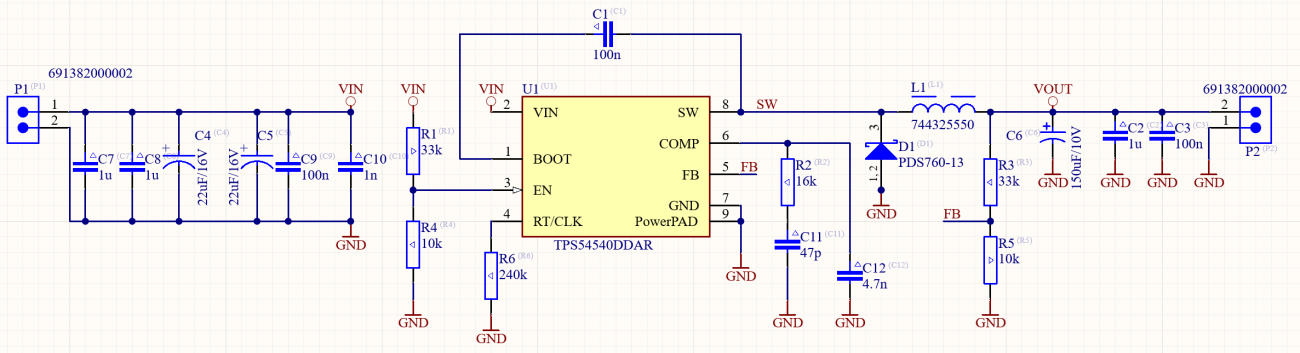
Figure 1.1. DC-DC converter schematic
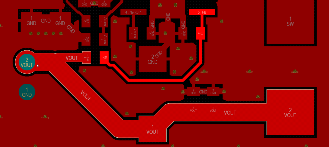
Figure 1.2. Correct PCB layout of the SMPS converter shown in Figure 1.1
Due to a layout modification error, the feedback trace was inadvertently connected within the main current path, using the same narrow trace width intended for the feedback signal. This change is illustrated in Figure 1.3.
As a result, the output current now flows through a narrow conductor, significantly increasing current density and introducing a voltage drop across the trace. Additionally, the feedback resistor in this flawed design was relocated and now is located away from the output connector further degrading the output voltage regulation at the converter output.
In this poor design, a 10-mil trace may conduct more than 5 A RMS, as the inductor ripple current also passes through it. Such conditions can easily lead to excessive heating and potentially a trace meltdown.
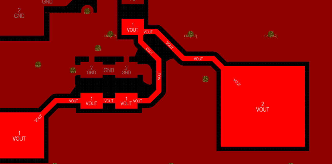
Figure 1.3. Incorrect PCB layout of the SMPS converter shown in Figure 1.1
This situation can be detected and analyzed directly within the PCB design phase. To illustrate this, let’s compare a well-designed layout with a poor one, focusing on three key aspects: current density, voltage drop, and power dissipation - all of which have a direct impact on the overall efficiency of the SMPS.
Correct PCB Layout Analysis
The current density in the output section of the SMPS design is shown in Figure 1.4, with a measured DC current density of approximately 60 mA/mil². The voltage drop developed across the VOUT trace, starting from the SMPS inductor to the output connector, is presented in Figure 1.5 and equals approximately 41 mV.
The corresponding power dissipation, considering only the DC output current, is calculated as: 5 A × 41 mV = 205 mW.
This represents the power loss on the output trace, which directly reduces the overall efficiency of the SMPS converter.
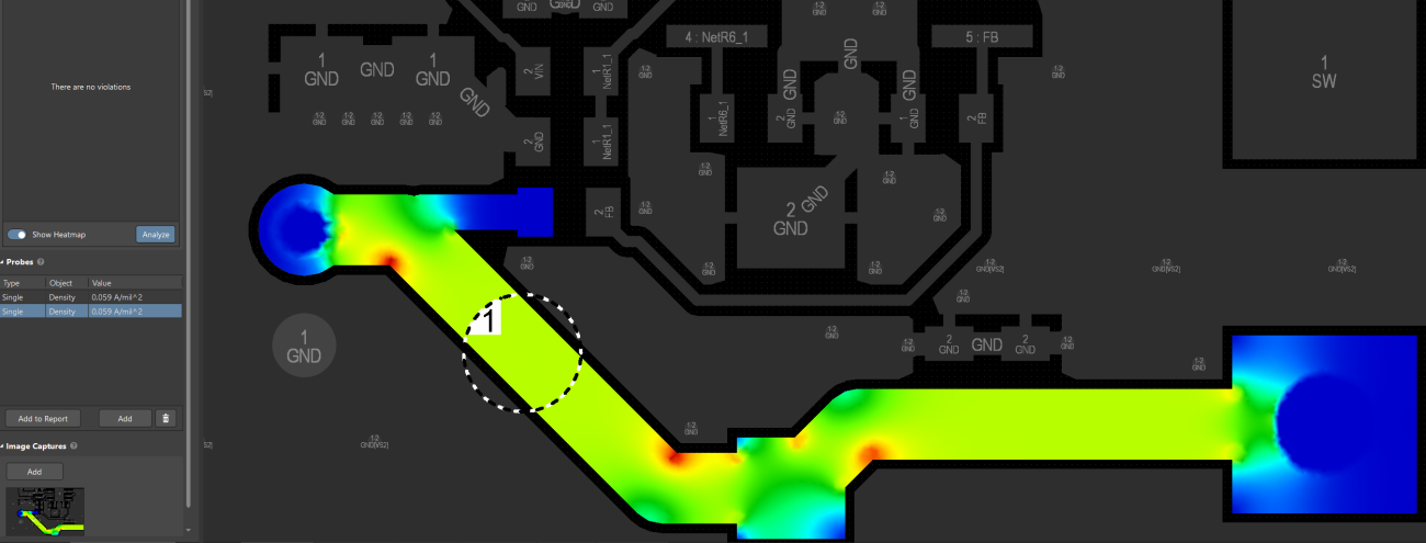
Figure 1.4. Current density on the output trace – correct PCB layout
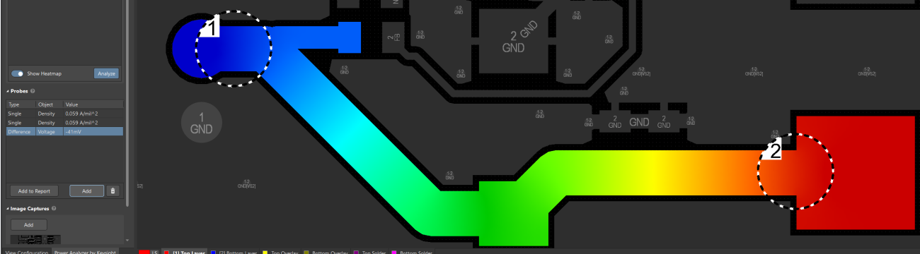
Figure 1.5. Voltage drop on the output trace – correct PCB layout
Poor PCB Layout Analysis
The current density distribution for the poorly designed layout is shown in Figure 1.6. Marker 1, placed on the narrow section of the output trace, indicates a current density of approximately 561 mA/mil² - nearly ten times higher than in the wider section near the output connector.
The voltage drop for this layout is presented in Figure 1.7. The DC current flow (excluding inductor ripple components) produces a voltage drop of 262 mV across the entire output path. The narrow section alone contributes approximately 236 mV of this total drop, as shown in Figure 1.8. The resulting power dissipation in the output trace is as follows:
- Total path: 262 mV × 5 A = 1.31 W
- Narrow section only: 236 mV × 5 A = 1.18 W
These losses are significantly higher than in the optimized layout and represent a substantial reduction in overall converter efficiency, as well as a potential thermal risk due to excessive heating.
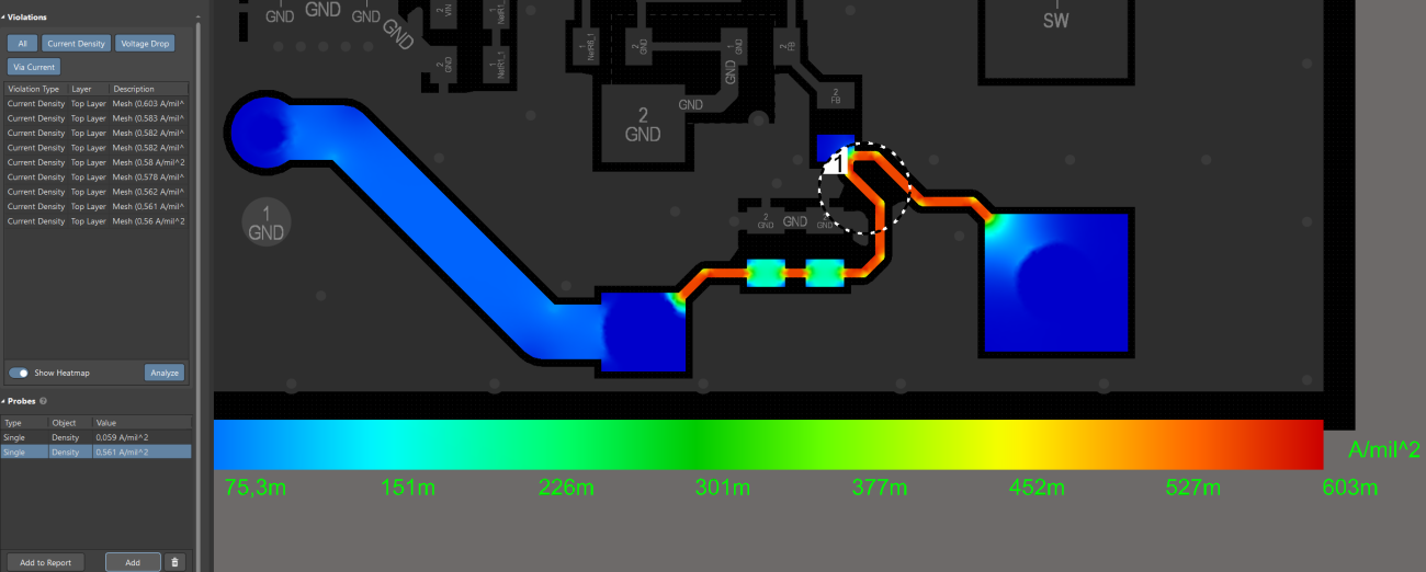
Figure 1.6. Current density on the output trace – incorrect PCB layout
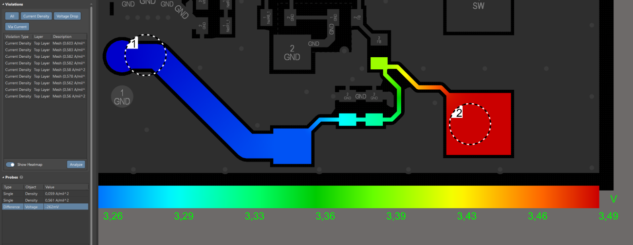
Figure 1.7. Voltage drop between the output connector and L1 inductor – incorrect layout
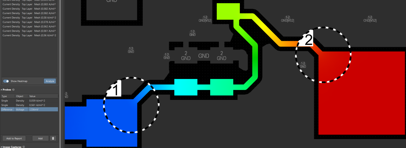
Figure 1.8. Voltage drop between L1 and C6 (main decoupling capacitor)
The narrow section of the trace may burn out due to excessive power dissipation during normal operation (as the nominal output current of the SMPS is 5A). Additionally, if the user accidentally short-circuits the output terminals, the resulting surge in current can easily exceed the safe operating limit of the trace. In such a case, the insufficient cross-sectional area of the copper may lead to meltdown and cause permanent damage to the device.
These issues can be prevented during the design phase by performing power integrity simulations using tools such as Power Analyzer by Keysight. By evaluating current density and voltage drop early in the design process, engineers can define realistic design constraints and validate them within the PCB layout - ultimately improving both reliability and power efficiency of the system.
Failure 2: Poor Signal Quality in Analog Designs
How can we ensure high quality of the analog signals processed in a circuit?
First and foremost, the analog section should be properly isolated from noisy digital circuits or switching power supplies (SMPS). This isolation does not mean galvanic separation; rather, it refers to separating the analog signal paths from those of the digital or power circuits that process data. To illustrate this principle, let’s consider a simple example of an RF low-pass filter with a cutoff frequency of 100 MHz. The schematic of this circuit is shown in Figure 2.1.
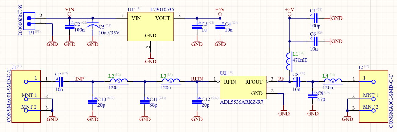
Figure 2.1. Schematic of an RF low-pass filter with a gain block
The low-pass filtering section is built using the following components: C10, L2, L3, C11, and C12 - these form the input filter stage that feeds the gain block U2. Additionally, C9 and L4 form another low-pass section at the output. A properly designed PCB layout should ensure that the return (ground) currents of U1 and U2 do not flow through the ground connections of the components forming the low-pass filter. If this condition is met, the processed signal will remain clean and free from interference generated by the active circuitry - particularly from U1, which is an integrated DC-DC converter and a potential source of switching noise. The poorly designed layout of this active filtering circuit is illustrated in Figure 2.2. Can you spot the problem in this design?
The input low-pass filter, located near the J1 connector, is referenced to a ground trace that originates at U1. This trace flows through the decoupling capacitors C1–C4 and C6, collecting switching noise from the converter. It then continues through C12 and C10, and finally connects to C5 (another decoupling capacitor). The ground trace then reaches C10, passes through vias to the bottom-layer ground plane, and from there, the return current travels toward the P1 power input connector.
Due to this poor routing, the ground potential for C10–C12 becomes noisy - the return current from U1 injects unwanted disturbances into the local ground of the filter. Consequently, the gain block (U2) sees its reference potential shifted by both AC and DC components, since the ground voltage at U2 differs from that at C11 or C12. This difference is caused by the finite conductivity of copper and the voltage drop developed by the return current flowing through the shared ground trace.
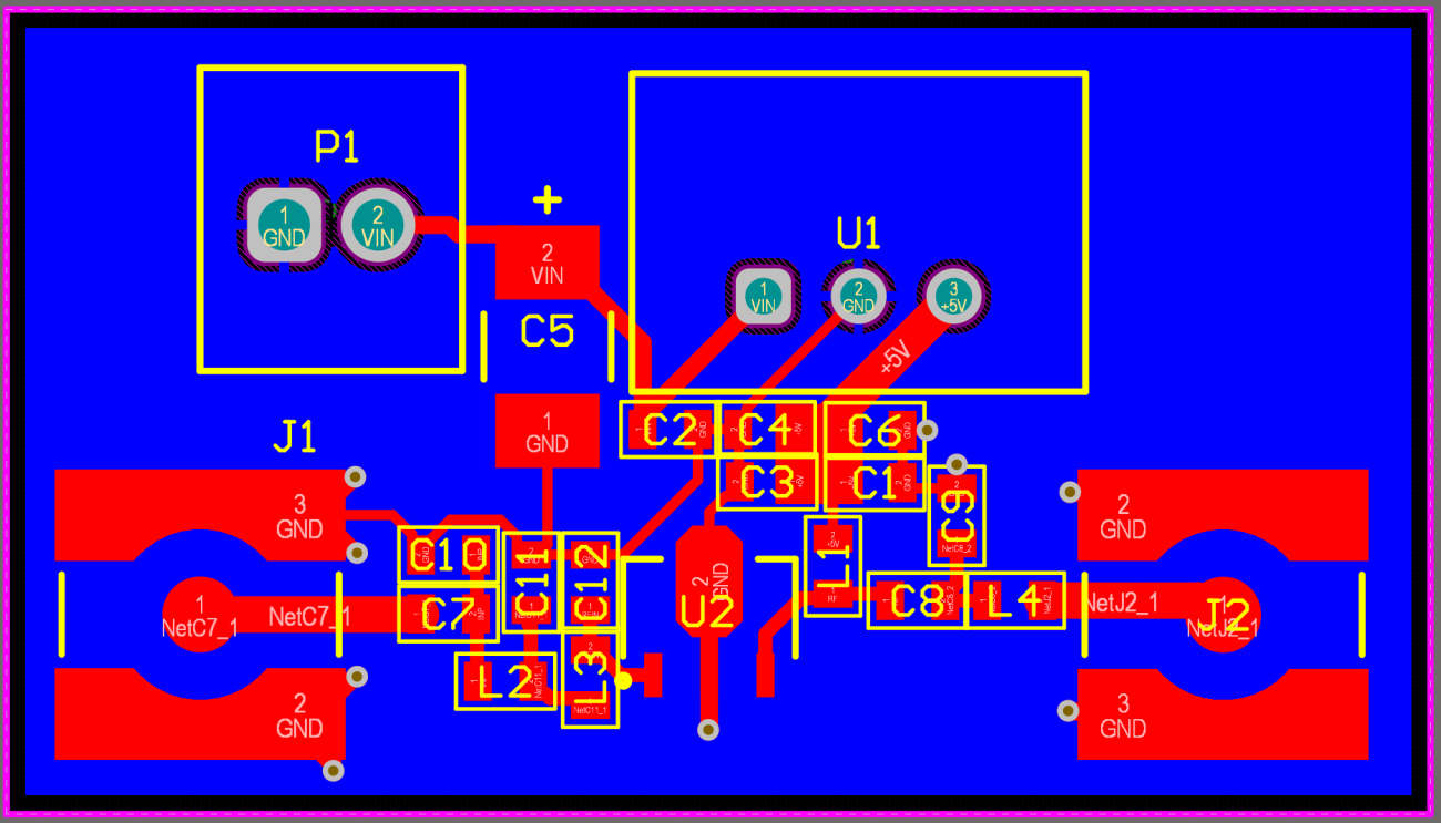
Figure 2.2. Low-pass filter PCB layout used for demonstration
The voltage distribution on the ground (GND) net is shown in Figure 2.3. Note that the voltage drop within this circuit reaches up to 275 µV (note that this also includes DC drop due to quiescent current of the gain block). Even though a solid bottom ground plane was used, the voltage drop still develops due to the incorrect routing of the ground return path. This example highlights that simply having a continuous copper plane does not guarantee low-noise performance if current return paths are not properly managed.
The Power Analyzer by Keysight can be used to perform such voltage distribution analyses and helps designers identify and correct grounding issues before fabrication, thereby improving the overall analog signal integrity.
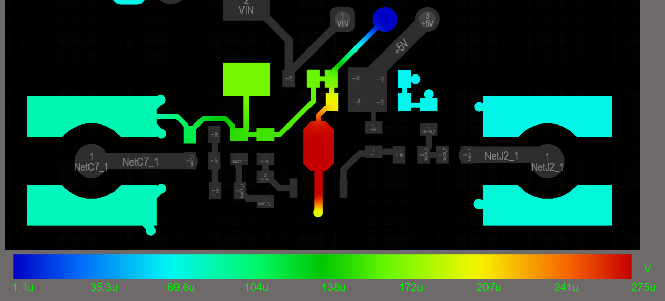
Figure 2.3. Voltage distribution on the GND trace (top layer)
How can this poor layout be corrected?
One effective approach is to stitch the low-pass filter section directly to ground and remove the GND trace that connects the SMPS stage to the filter. The filter’s ground should instead be tied directly to the ground reference of U2, ensuring a clean and stable return path for the analog signal. Additionally, a cutout in the bottom-layer ground polygon can be introduced to prevent return currents from U1 and U2 from flowing through the filter section. This modification isolates noisy power currents from the sensitive analog paths.
The updated PCB layout is shown in Figures 2.4 (top layer) and 2.5 (bottom layer). The corresponding voltage distribution, presented in Figure 2.6, clearly demonstrates that the ground voltage gradient is significantly reduced, confirming the improved grounding strategy and overall signal integrity.
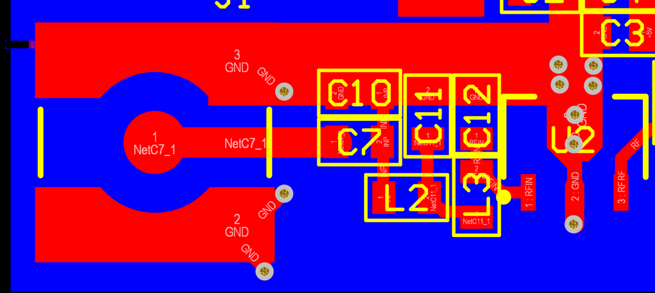
Figure 2.4. Updated layout (top layer) – GND section of the low-pass filter isolated from return currents of U1 and U2
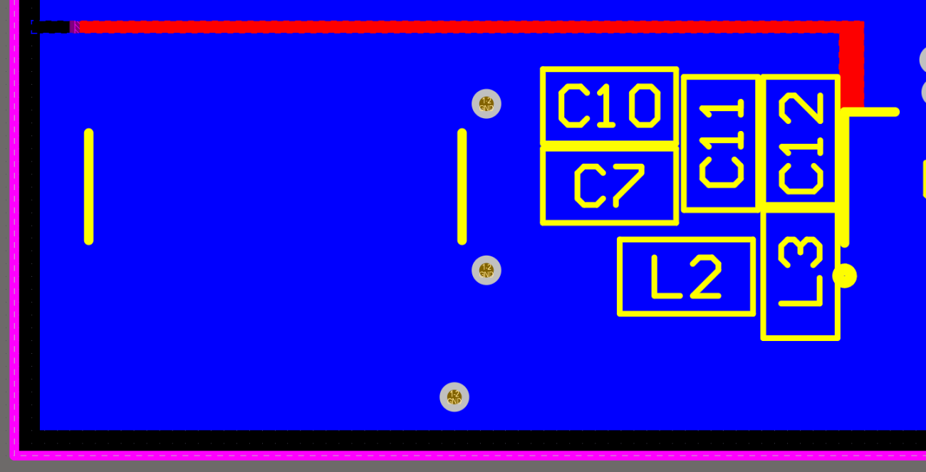
Figure 2.5. Updated layout (bottom layer) – GND section of the low-pass filter isolated from return currents of U1 and U2
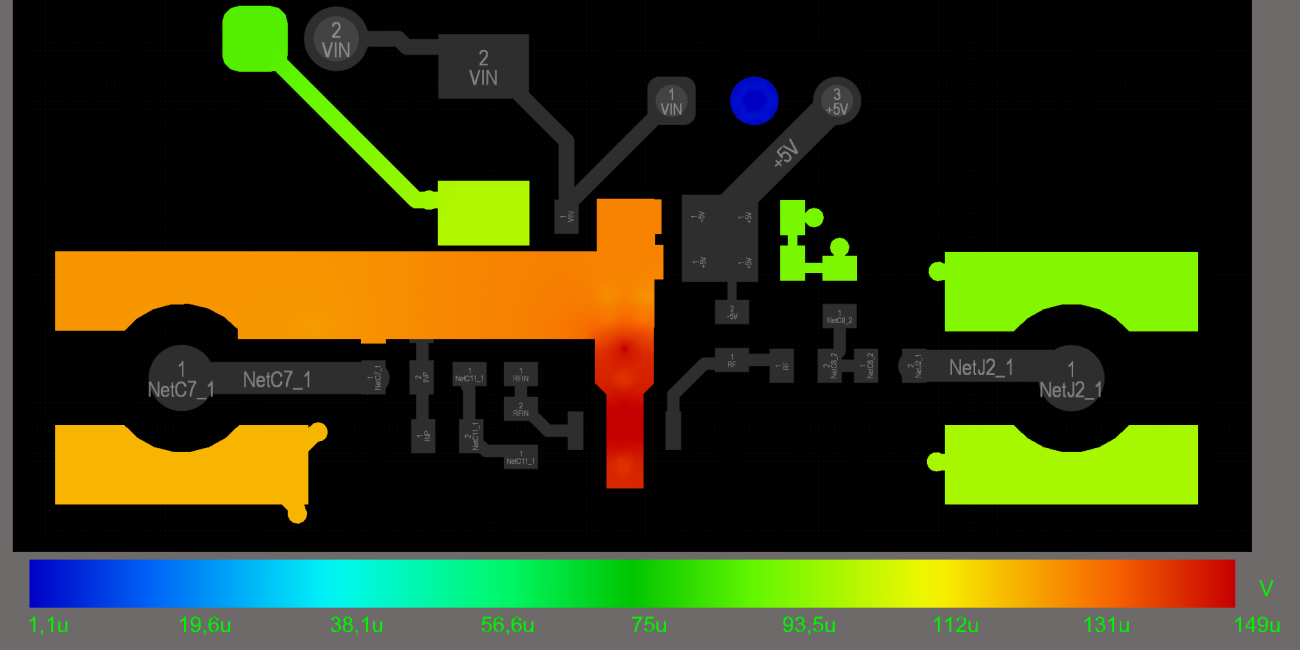
Figure 2.6. Voltage gradients on the updated PCB layout
Failure 3: Instabilities in SMPS Converters
Switch-mode power supply (SMPS) designs combine power stages and analog control circuitry. The power stage is responsible for driving either external MOSFETs or internal switches within the IC, and it handles high currents and high dV/dt voltages associated with the output voltage and power delivery to the load.
An example of the power stage components in a typical DC-DC converter is shown in Figure 3.1, where the power stage is highlighted with red rectangles.
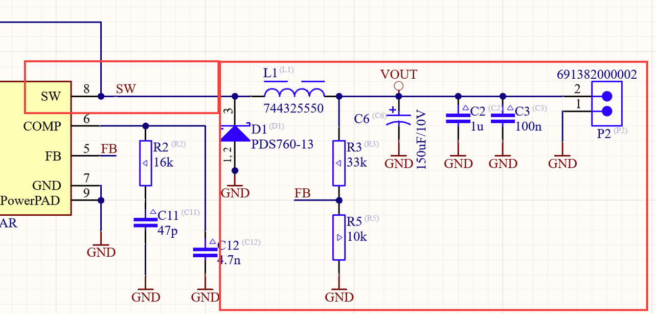
Figure 3.1. Power stage of the DC-DC converter
On the other hand, the analog sections of an SMPS converter typically include an error amplifier organized around the feedback loops - either current and voltage loops in current-mode controllers or a voltage loop in voltage-mode controllers. A compensation network is also required to ensure stable operation.
In Figure 3.2, the analog circuitry of the SMPS converter is highlighted with red rectangles. Note that these sections are connected to the GND net, which is shared with the power stage, making proper grounding and layout critical for overall stability.
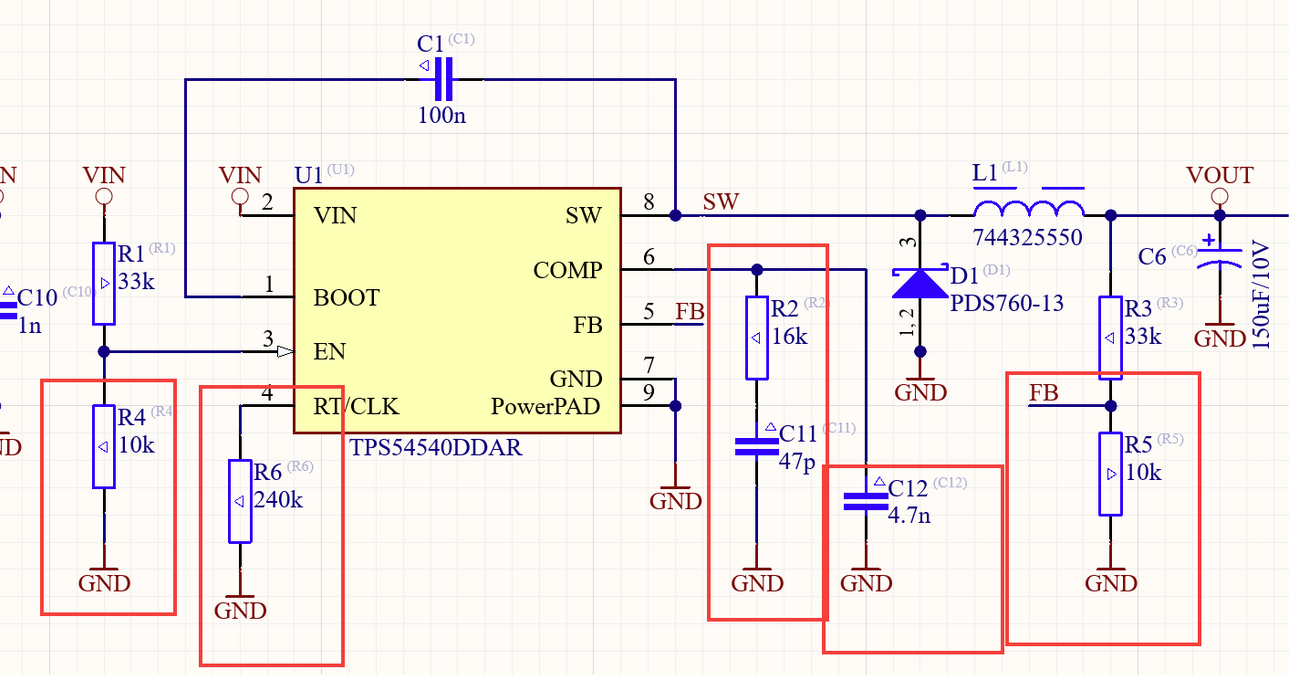
Figure 3.2. Analog circuitry of the DC-DC converter
The components of these analog sections should be placed on the PCB in such a way that the high-current paths of the power stage do not flow through the analog circuitry, particularly through the shared ground path. If this rule is not followed, the SMPS may exhibit several issues, including:
- Poor voltage regulation, correlated with output current at the load
- Excessive voltage ripple on the output
- Audible noise due to instability in the feedback loop(s)
- EMC emissions above acceptable levels
- Reduced efficiency resulting from control loop instability
- Additional problems caused by switching frequency instability, such as significant heating of the main power inductor
A current path analysis can be conducted during the PCB design phase to identify and prevent such issues before fabrication. An example of this approach is presented in the section related to Failure 2 (see Figures 2.3 and 2.6). Designers are encouraged to perform similar analyses in their own projects, ensuring that voltage gradients across analog components remain unaffected by return currents - particularly those generated by the switching operation of the converter.
Conclusions
Three PCB design failures have been presented in this article, each capable of significantly impacting circuit performance - from reduced SMPS efficiency and degraded analog signal integrity to potential instability or even PCB trace burnout. The risk of such issues can be greatly minimized during the design phase by incorporating voltage drop and current density analyses using tools such as Power Analyzer by Keysight, enabling designers to identify and correct potential problems before production.
However, tools alone can’t ensure consistent design quality across an organization. To gain the full benefit (and ensure consistent quality across projects) you need structured collaboration, repeatable workflows and accountability across ECAD, MCAD, and system teams. That’s where Altium Agile Teams comes in. Using this solution you can turn each power-integrity insight into a tracked task, standardized fix, and shared organizational knowledge base.
Start with Agile Teams Eval Flow here: Get Started

About Author

Related Technical Documentation

Table of Contents
- Failure 1: PCB Trace Meltdown
- Correct PCB Layout Analysis
- Poor PCB Layout Analysis
- Failure 2: Poor Signal Quality in Analog Designs
- How can we ensure high quality of the analog signals processed in a circuit?
- How can this poor layout be corrected?
- Failure 3: Instabilities in SMPS Converters
- Conclusions
Get the full Power Analyzer Experience
- Test PI insights together with real-time collaboration and structured workflows.
- Your Agile Teams evaluation includes full access to Power Analyzer.
Contact Us
Thank you, you are now subscribed to updates.

