


Chemical Processes Could Make Semiconductor Manufacturing More Sustainable


Although essential to modern life, semiconductor manufacturing is energy- and resource-intensive, demanding higher consumption of electricity, water, chemicals, and process gases, all of which contribute to greater energy use and environmental impact—an unfortunate reality that is further compounded by the increased complexity of advanced chip manufacturing and increased demand.
"If the current growth path were to continue unchecked, carbon emissions from semiconductor production would rise by about 8% annually in coming years and not peak until about 2045," says The Boston Consulting Group.
In response to these challenges—and increased pressure as governments worldwide begin to implement stricter environmental regulations—the semiconductor industry has been targeting innovation initiatives and research and development efforts toward more environmentally friendly processes. Alternative solutions have started to gain traction.
Here, we delve into the key challenges companies face, how chemical processes are evolving to make semiconductor production more sustainable, and the industry leaders that are spearheading the transition.
Critical Challenges in Achieving Sustainability
|
Global Warming Potential (GWP): a measure of how much heat a greenhouse gas traps in the atmosphere over a specific period (typically 100 years) relative to carbon dioxide (CO₂). Gases with a higher GWP contribute more to global warming. |
One of the biggest hurdles to making semiconductor manufacturing more sustainable is the fact that many of the chemicals used in production are both essential to the process and hazardous to the environment. Although necessary, if not properly managed, these substances are often toxic and pose risks to human health and the environment. The waste generated from these chemicals can also be difficult to dispose of, leading to further environmental challenges.
The semiconductor industry has faced criticism for its significant environmental impact, mainly due to the release of high GWP gases and its substantial water and energy consumption. While these chemicals are essential for the functionality and performance of semiconductors, we only need to glance a short while back to fully appreciate their environmental consequences.
In the 1970s through the 1990s, when the United States was a dominant force in semiconductor production, the environmental hazards associated with fabrication plants were not widely recognized. During this period, Silicon Valley, home to numerous fabs, became the site of several Superfund locations—areas so contaminated that they were placed on the National Priorities List for federal cleanup. For instance, at an Intel site active between 1968 and 1981, the EPA identified more than a dozen contaminants in the groundwater, including arsenic, chloroform, and lead.
Although the industry now takes an aggressive, proactive stance on sustainability, these events underscore the imperativeness of balancing technological advancement with environmental stewardship.
The Role of Chemicals in Semiconductor Manufacturing
Semiconductor fabrication involves various chemical processes crucial for etching, cleaning, doping, and patterning materials. While necessary for producing high-performance chips, these chemicals often come with significant environmental drawbacks, including hazardous waste and greenhouse gas emissions. For example:
Etching: Removing layers of material from the wafer surface to create the intricate patterns that define a chip's functionality. Perfluorocarbons (PFCs) used in etching processes are nearly impossible to replace due to their effectiveness in creating the detailed structures needed for advanced microchips. Unfortunately, these gases have a GWP thousands of times higher than carbon dioxide, making their impact on climate change disproportionately large.
Cleaning: Wafers must be meticulously cleaned at various stages to remove impurities. The use of solvents, acids, and bases is integral to achieving the extreme levels of purity required for semiconductor devices. Unfortunately, these chemicals are often hazardous and create a significant waste stream.
Doping: The process of adding impurities to semiconductor material to alter its electrical properties. Chemicals like arsine and phosphine, which are highly toxic, are commonly used in doping.
Innovations in Chemical Processes for Sustainability
Recognizing the environmental impact of these chemical processes, the semiconductor industry is increasingly exploring alternatives and innovations to make production more sustainable. Here are some of the most promising developments:
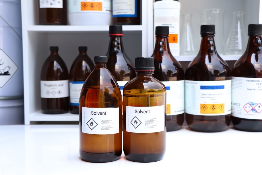
- Greener Solvents and Cleaning Agents
One of the key areas of innovation has been the development of greener solvents and cleaning agents that have a lower environmental impact. Traditional solvents like isopropyl alcohol, while effective, can be hazardous in large quantities. Manufacturers are now researching alternative solvents that are biodegradable and less toxic, reducing the harmful effects of cleaning processes on the environment.
For instance, companies are exploring the use of aqueous-based cleaning solutions that use water as the primary solvent. These solutions can effectively clean wafers while drastically reducing the need for harmful chemicals. Additionally, new cleaning agents are being developed that can be recycled and reused, significantly reducing chemical waste.
Chemicals of high concern in semiconductor cleaning are N-methyl pyrrolidone (NMP) and tetramethylammonium hydroxide (TMAH), as well as the commonly used solvent dimethyl sulfoxide (DMSO). Hence, companies like Merck KGaA are reformulating and introducing new products that use less toxic, safer chemicals without using NMP, TMAH, or DMSO.
- Reduction in High-GWP Gases
Researchers are working on developing alternative gases with lower GWPs that can still achieve the precision required in etching processes. For instance, nitrogen trifluoride (NF3) has been introduced as a substitute in some applications, as it has a lower GWP than traditional PFCs.
Additionally, improvements in process equipment can help reduce the amount of gas used during etching, thereby lowering emissions. Advanced etching techniques that use plasma-based processes are also being explored. These methods can significantly reduce the quantity of harmful chemicals required, contributing to a more sustainable production process.
More on the transition from PFCs to NF from The Semiconductor PFAS Consortium.
- Closed-Loop Chemical Recycling Systems
Another promising innovation is the adoption of closed-loop chemical recycling systems, which allow manufacturers to reuse chemicals rather than dispose of them after a single use. This is particularly important for chemicals used in cleaning and etching processes, as they account for a large portion of the waste generated in semiconductor manufacturing.

By using advanced filtration and purification technologies, manufacturers can reclaim and reuse chemicals, reducing both waste and the need for raw materials. This not only cuts down on environmental impact but also lowers operational costs, creating a win-win scenario for manufacturers.
To address the rising demand for raw materials as manufacturing processes advance, TSMC collaborated with suppliers to initiate the "Electronic-grade Chemicals Recycling Project." This initiative focuses on developing technology to recycle process waste materials, converting them into electronic-grade products for reuse at TSMC, thus enhancing the value of TSMC's closed-loop recycling model. In 2023, cyclopentanone waste was successfully refined into electronic-grade cyclopentanone that met TSMC's stringent quality standards. This reprocessed chemical was officially introduced in November at TSMC's AP3 advanced packaging and testing facility and is expected to reduce annual liquid procurement by 750 tons and cut carbon emissions by 380 tons, exemplifying green manufacturing and advancing environmental sustainability.
- Dry Processing Techniques
Dry processing techniques have been developed to reduce water usage and waste generation. These techniques, such as dry etching, eliminate the need for liquid chemicals by using gases or plasmas instead.
Dry etching, in particular, has played a significant role in the transition to more sustainable options, eliminating the need for toxic chemicals and lowering water consumption. Plasma-based cleaning methods are also gaining traction, offering similar benefits by using less water and energy compared to conventional wet cleaning methods.

Industry Efforts and Global Impact
In response to growing environmental concerns, semiconductor companies are increasingly investing in strategies to reduce their manufacturing operations' environmental impacts. According to Deloitte, these companies are focusing on adopting manufacturing processes that utilize materials with lower GWP. This includes retrofitting existing plants and building new facilities to incorporate processes that rely on chemicals and gases with lower emissions.
Traditional semiconductor manufacturing heavily uses gases with high GWP, such as PFCs, hydrofluorocarbons, nitrogen trifluoride (NF3), and sulfur hexafluoride. Unfortunately, up to 80% of these fluorinated gases are often released into the atmosphere after processing. PFCs are hard to replace, but progress is being made. For instance, Samsung Semiconductor is developing process gases with lower GWP to replace PFCs in key manufacturing steps like etching and chemical vapor deposition, having already implemented these in several products since 2018. Similarly, Tokyo Electron Limited (TEL) introduced a high-aspect ratio etch process that operates at cryogenic temperatures, uses alternative chemicals, and significantly reduces both energy consumption and greenhouse gas emissions.
While these efforts are promising, Deloitte notes that transitioning to alternative gases is a slow process that often results in incremental improvements.
The Path Forward
By transitioning to greener alternatives wherever possible and optimizing usage, manufacturers can reduce their carbon footprint, mitigate the ecological impacts of their operations, and make progress toward their carbon commitments. The aforementioned innovations in greener chemicals, dry processing techniques, and closed-loop recycling systems represent critical steps toward a more sustainable future for the industry.
While challenges remain, the growing commitment from industry leaders and the increasing availability of new technologies provide hope for a more earth-friendly semiconductor manufacturing process. As companies continue to invest in sustainable solutions, the industry is poised to make significant strides in reducing its environmental impact, ensuring that the chips powering our modern world are produced in a way that is more in harmony with the planet.

About Author
Related Resources
Related Technical Documentation
Table of Contents
Design to Release, Without the Friction
- Keep reviews tied to the right version
- Reduce handoff confusion and rework
- Spot sourcing and release risk earlier
- Work solo, share when needed
Get Started
Thank you, you are now subscribed to updates.