


The Current State of AI in PCB Design in 2023


Your favorite machine learning, optimization, and generative AI algorithms may soon be used in your favorite PCB design program. Now that ChatGPT has become a household name and competitor companies are developing their own GPT equivalents (Claude, LLaMa, etc.), EDA startups are looking at how to leverage these tools to help PCB designers and engineers be more productive. With so many industries touched by automation and AI, it was only a matter of time before PCB designers would get their own tools.
Where AI is Being Applied in PCB Design
PCB design involves a multitude of tasks, ranging from circuit design to PCB layout and preparation for production. As of 2023, there is no single system that will handle all of your engineering and PCB design tasks. But the range of options available today is impressive, both in the design and manufacturing space.
ChatGPT and Other Chatbots
Because ChatGPT is the elephant in the room when it comes to generative AI, it’s worth mentioning what it can do and how people are trying to use it. Other chatbots have essentially the same capabilities, so the tasks below can also be performed on these platforms. On this blog, myself and others have shown where ChatGPT could be useful for some targeted design tasks:
- Component selection or descriptions - Accuracy here varies wildly, but plugins are helpful for providing specific information or datasheet (see here). There are millions of components, and an AI-driven supply chain with tagged data could help with part selection.
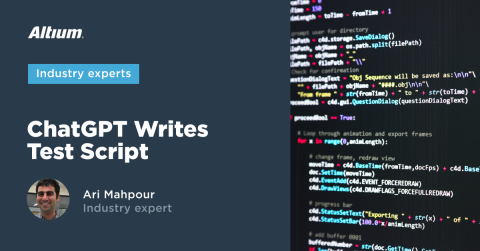
- Code or script generation - Writing code or scripts is one of the classic use cases of ChatGPT, including Altium scripts.
- Automated testing - Ari Mahpour has shown how to use the generative capabilities in ChatGPT for automated testing of embedded systems, read more here.
- Basic calculations - If you don’t have formulas memorized, you can always query ChatGPT for the formulas or for an example calculation.
- Datasheet questions using plugins - Internet search features allow users to pass datasheet URLs to a chatbot, so you can now use information from datasheets in other prompts.
Today, the internet search plugins available on ChatGPT and the similar search plugins on other systems are a big change that help you expand the scope of information you can analyze. For electronics designers and PCB designers, the biggest use case is the last point I mention above: analyzing datasheets. This hugely expands the scope of what you can do in a generative platform.
Generation from System Requirements
Another AI-driven approach that implements code to automate front-end system-level design comes from JITX, a Nexar Partner. JITX takes a code-based approach to developing circuits and outputs a project in Altium’s file format. While not prompt-based, it is using AI in its system to generate the front-end CAD inputs and take a designer through an important portion of the design process. There is still human-in-the-loop as the CAD outputs need to be inspected and verified against constraints prior to routing.
To learn more, watch our recent OnTrack Podcast episode with Duncan Haldane, founder and CTO of JITX.
Visual Inspection and Traceability
On the manufacturing side, innovative vision systems on the manufacturing line are using AI to inspect component placements and enable traceability throughout the supply chain. Ultimately, if a recall is required, it could be targeted to a specific board lot or component lot from a specific factory, rather than an entire Rev of a design. This is where Cybord.ai is working; their AI-enabled vision-based system works on the manufacturing line to identify components and even reject placements if a part is suspected to be counterfeit.
Once problems are identified with this type of system, the feedback needs to reach directly to the design team so they can update the design in a future revision. This is a vital element of quality control that is mostly manual today. To learn more, watch our recent OnTrack Podcast episode with Dr. Eyal Weiss, founder and CTO of Cybord.ai.
Looking to the Future: Generating CAD Data
I still think the future of AI in PCB design is direct generation of CAD data, including in the PCB layout. This could include generative placement of components, such as in groups (e.g., using the Rooms feature) as well as in critical spots for mechanical, thermal, or UX reasons. Once placed (both generatively and manually), your AI-based autorouter comes into play to route specific parts of the design. Finally, having a human-in-the-loop approach to qualify the outputs enables reinforcement learning so that only the best results remain part of the training set.
Reinforcement Learning in Generative PCB Design
In my opinion, and in the opinion of other startups, a reinforcement learning approach is the best option for building AI-driven PCB design models. Any portion of a design that has some data associated with it (which is everything in a PCB layout) or that can be categorized can be used to build an AI model for PCB design.
AI-driven PCB design takes two components: building models and design optimization. Model building is all about creating a numerical model relating features in a PCB layout (component placement, routing, etc.) with design performance metrics, such as:
- Power integrity specifications
- Signal integrity specifications
- Power output/consumption
- Types of interfaces present in the design
- How each layer is used
The more tagging applied to the design, the better. The biggest front-end task is categorizing and tagging your designs so that the training data is consistent to certain design domains. For example, if you want to generate a switching power supply layout, you shouldn’t use a single-board computer as training data!
Once you have a generative model for a PCB domain, the system can generate CAD data and this can be examined by the PCB designer to verify placement, routing, constraints, and mechanical form factor. After tweaking the design manually, the design can be put back into the training set. One way to Integrate modeling with optimization within a reinforcement learning method is outlined below.

- Training: Data is input into a training dataset and is used to build a prediction model for a specific aspect of the PCB layout. This aspect could be the arrangement of circuit blocks, layer stackups, routing decisions, or other features.
- Generated PCB data: The model can then be used to generate CAD data that attempts to conform to the constraints (PCB design rules) specified by the PCB designer. This could be placement or routing.
- Human evaluation: A human designer would need to go back and check the results to ensure constraint conformance and manufacturability. This could involve manual inspection, simulation, etc.
Once a design is generated, evaluated, modified, and accepted, it can be added back into the training set as a new input. This reinforcement learning process allows the generative model to be continuously updated and tuned with acceptable designs.
As these design tools and workflows develop, rest assured that we'll be there to guide you through the brave new world of AI-driven PCB design. No matter what kind of product you need to design and build, make sure you use the complete set of PCB design features in Altium. To implement collaboration in today’s cross-disciplinary environment, innovative companies are using Altium to easily share design data and put projects into manufacturing.

About Author
Related Resources
Related Technical Documentation
Table of Contents
Design to Release, Without the Friction
- Keep reviews tied to the right version
- Reduce handoff confusion and rework
- Spot sourcing and release risk earlier
- Work solo, share when needed
Get Started
Thank you, you are now subscribed to updates.

