From Pads to Altium: Evaluation Resources to Help You Switch
As you dive into your evaluation of Altium Designer, I wanted to share with you some information specifically for someone like you that is coming from a PADS background.
When we look at what engineers and designers really do every day, we often see that as much as 61% of your day can be consumed with non-design related tasks.
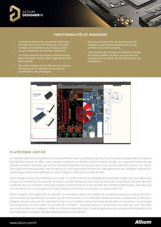
These tasks are a byproduct of using a collection of tools (toolchains), vs. the Altium Designer paradigm of using a Unified Design Environment. So, as you get into your evaluation the attached guide will highlight for you the areas that our customers realize the biggest improvements when moving to Altium Designer vs. where you are coming from.
While you will need to familiarize yourself with the discrete technology within Altium Designer, I do ask that you focus on the true value of what Altium Designer can do for you. Of note:
- Elimination of the ad hoc processes associated with using a toolchain design approach.
- No longer being forced to manually curate and then find design data for released products, WIP, Library and Supply Chain information.
- Get rid of the intermediate files when collaborating with your MCAD counterparts
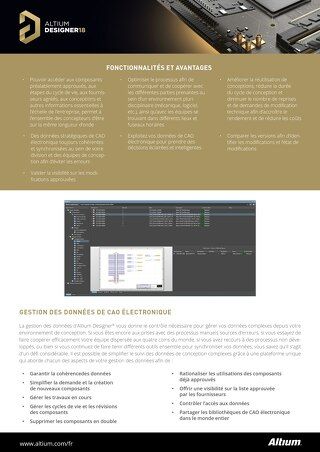
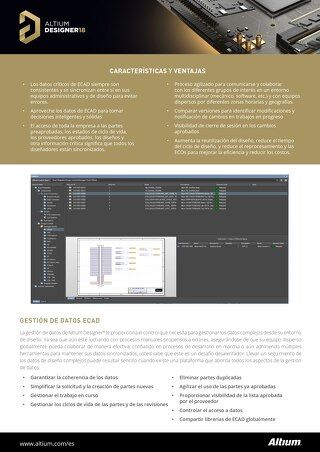
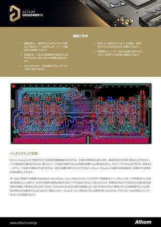
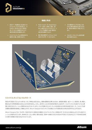
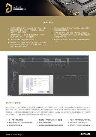
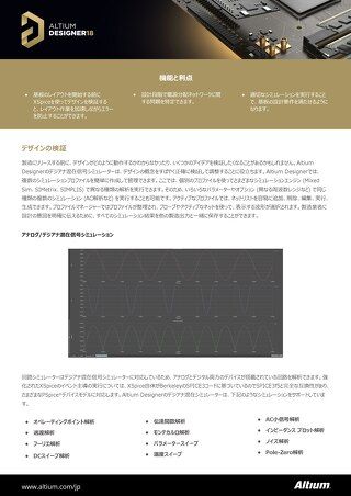
Get started now with our Guidebooks resources:
Once you have had the chance to review our Guidebooks, start your Design Quest journey with Altium Designer in this series of interactive videos from our Altium Designer Evaluation Guide. By following the interactive videos in the guide, we will take you from our user interface fundamentals to choosing a library strategy all the way to the end of your design journey with the powerful release management tools in Altium Designer.
