Circuit CAD Software for PCB Design


Key Takeaways:
- Unified Workflow: Modern hardware development requires moving seamlessly from schematic capture to PCB layout without losing data.
-
Simulation First: Running signal integrity simulation and power supply simulation during layout prevents costly respins.
-
Collaboration: Real-time ECAD MCAD integration is not optional; it's required to fit complex boards into tight enclosures.
Circuit CAD Software for PCB Design Hardware is hard work. Unlike software, you can't just "patch" a physical board once it's manufactured. Whether you are a hardware engineer working on a complex rigid-flex PCB design or a student looking for a 3D PCB design software free download to learn the ropes, the tool you choose dictates your success.
The best PCB CAD tools function as complete PCB design data management systems. They integrate schematic capture software with physical layout and the final design review process, ensuring that design intent is preserved from the first logic gate to the final fabrication file.
An Introduction to Circuit CAD Tools
Circuit CAD tools are the cornerstone of PCB design. These tools give you the capability to create schematics and a circuit board layout of your new product, but not all CAD features are created equal. Today’s designers need to take a comprehensive approach to PCB design that includes mechanical design, simulation, and preparation for manufacturing. Your productivity stays high when your CAD tools are integrated with more advanced design features and your other design tools, and you can quickly design PCBs for advanced applications.
To handle the complex challenges of a complete design project, you need a complete circuit CAD system for PCB design. Altium Designer, available within Altium Develop, offers all these advantages and many more in a single program. You’ll have everything you need to design your next PCB in a single program, including tools for MCAD collaboration in popular mechanical design applications.
If you’ve got a great idea for a new electronic device, you’ll need to turn it from a circuit diagram into a schematic. Later, you’ll need to turn your schematic into a layout, and then you’ll need to turn your layout into an actual PCB. The challenges of today’s complex designs require professional quality computer-aided design software tools. Too often in the past designers were forced to choose between settling for lesser quality tools, or mixing together tools from different systems in order to get the job done.
When all your design and production planning tools are integrated into a single application, you won’t have to worry about incorporating a third-party application into your design workflow. Altium Designer is a complete CAD software with a PCB design system that will give you the resources you need for your greatest design challenges. From your initial schematic capture to your final manufacturing output data, all the tools you need for printed circuit board design are available in Altium Designer.
The Role of Circuit CAD Tools in PCB Design
CAD circuit design tools in your PCB design software do more than just allow you to place components on a board outline. Simpler circuit CAD software will give you these capabilities, but not much else. PCB CAD tools should not be limited to component layout in 2D board designs. Working with more advanced board configurations like rigid-flex design takes CAD tools that link multiple boards into a single device. The best CAD tools create a link between multiple layers on your board, allowing routing through vias and within the inner layers. Modern CAD circuit design tools give you a full view of your device and allow you to approach your design holistically.
The best CAD software for PCB design will interface with a comprehensive set of design rules. These design rules govern the function of your routing features, simulation tools, and features for generating manufacturer deliverables. A rules-driven design engine in your circuit CAD software will automatically show you when you’ve created a rules violation, allowing you to fix any problems before you send your board off for manufacturing. A great CAD module forms the foundation for designing your next PCB, regardless of the application.
Mastering the PCB Layout Design Steps
A professional PCB design workflow follows a strict "V-Cycle" of verification, managing constraints from the initial concept through to manufacturing.
- Advanced Schematic Capture: Schematic capture software links directly to live supply chain data and defines PCB design constraints (such as high-voltage clearances for a 12V power supply PCB layout) at the logic stage. This ensures rules are propagated forward rather than applied retroactively.
- Constraint-Driven PCB Layout: During PCB layout design, the software automatically enforces the rules defined in the schematic. This is critical for high speed PCB design, where trace length matching must be exact to preserve signal timing.
- ECAD MCAD Integration: What is MCAD software’s role in electronics? It allows for the precise alignment of mechanical and electrical components. Tools like Altium Designer synchronize 3D models between domains, ensuring your power supply PCB layout design fits inside the enclosure and connectors align without the need for physical prototypes.
The Basic PCB Design and Circuit Layout Tools You Need
Your schematics define the basic structure of your device and provide the intimate details on how your components and power/ground lines are connected together in a coherent structure. Your new PCB starts its life in a powerful schematic editor, where CAD circuit tools are used to place and connect components together in a real device. The best schematic editors will include a SPICE-based simulator to evaluate the functionality of your circuits.
Once you finish your schematics, you’ll need to use a schematic capture utility to place your components into an initial PCB layout. You’ll then use CAD tools to arrange and route components together into a complete circuit board. The full layout of components on your PCB should feed directly into simulation and analysis features so that they can access information directly from your circuit CAD PCB design. Accurate PCB layouts help ensure your manufacturer can build your board properly on the first production run, which prevents fabrication delays and redesigns.
- All designs start with schematic capture in your ECAD software. The best schematic design end editing features will include access to libraries you can use to find and place components into your schematic sheets.
Learn more about using your design software for schematic capture. - Hierarchical schematic design is a great way to keep each part of your device organized as it becomes more complicated.
Learn more about the difference between flat and hierarchical schematics. - Whether you’re designing a single multilayer board or a complex multi-board system, you need the right circuit CAD tools to complete your PCB layout.
Learn more about using your circuit CAD tools for advanced PCB design.

Altium Designer’s powerful hierarchical schematic editor
Design Tools in Advanced CAD Software
Most freeware and online circuit CAD platforms include schematic editing, capture, and layout features, but they don’t include more advanced features. You’ll be forced to add other programs to your workflow if you want to understand your circuit board’s behavior and prepare for full-scale manufacturing. Post-layout simulation features are important for predicting signal integrity problems like crosstalk and ringing, and a set of advanced simulation features will calculate these important effects directly from your layout.
In addition to these important simulations and analysis features, manufacturing preparation requires generating important documents directly from your PCB layout files. Your manufacturer will need Gerber files, assembly drawings, bills of materials, and more in order to get your board into production. In addition to these important circuit CAD and manufacturing features, you need a set of MCAD tools as part of enclosure design for your new product.
High-Speed PCB Design Guidelines & Analysis
As devices get faster, signal integrity analysis in PCB design becomes non-negotiable. If you are working on high frequency PCB design or modern interfaces like DDR5 or USB-C, you need tools that can handle physics-based constraints.
Critical Features for High-Speed Design:
- Differential Pair Routing: Routing high-speed signals requires precise differential pair routing guidelines. Your software must allow you to tune trace lengths in real-time to match phase and impedance. Pro Tip: Always route differential pairs together to reject common-mode noise.
- EMI & Crosstalk: EMI PCB layout design prevents your board from acting like an antenna. Features like 3D electromagnetic simulation help visualize return paths and shield sensitive analog signals from noisy digital switching.
- Impedance Control: A correct PCB layer stackup is the foundation of signal integrity. Your CAD tool should include an impedance calculator to determine the exact trace width needed for 50Ω or 90Ω (USB/SATA) routing.
Example: SATA PCB Layout Guidelines When routing legacy or modern storage interfaces (like SATA), you must maintain a strict 100Ω differential impedance. A professional PCB layout designer uses design rules to flag any segment that deviates from this impedance, ensuring data isn't corrupted during transmission.
Why You Need MCAD Capabilities in Your PCB Design Software
Advanced products with complex mechanical requirements take more than just ECAD tools. Including MCAD capabilities in your PCB design process gives you a full 3D view of every aspect of your design. You’ll be able to see how your product looks before it comes off the assembly line. You can verify enclosure dimensions, clearances, and the overall arrangement of components on your board. You can even get a 3D view of your trace layout and routing.
If you use proprietary components or nonstandard components, you’ll need to include footprints and STEP models as part of the mechanical design process. The right PCB design package allows you to link STEP models to your components as part of your design process. If you’re working on rigid-flex boards or a multi-board system, using MCAD software takes the guesswork out of design and helps ensure your boards will meet your packaging requirements.
- When people from different teams are contributing to a new product, proper collaboration is the key to design success. Altium Designer helps you create a complete product development workflow centered around PCB design.
Learn about the basics of team collaboration. - Simple mistakes can arise that cause component placement errors when your ECAD and MCAD software siloes your design teams.
Learn more about preventing design errors with integrated ECAD/MCAD software. - Integrated ECAD and MCAD software lets you use STEP models from other design programs. This collaboration and data management is easy.
See how managing 3D STEP models improves productivity and collaboration.
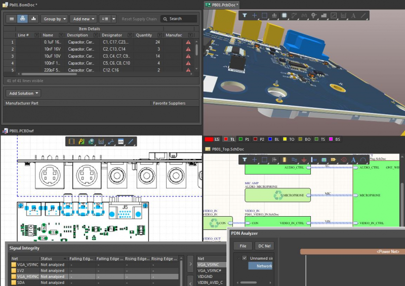
You’ll find multiple circuit CAD tools in Altium Designer
A Unified Design Environment in One CAD Software Download
As PCB design software offers more capabilities to designers and engineers, CAD PCB design tools can no longer sit separated from simulation, visualization, and manufacturer deliverable generation tools. The new PCB design paradigm unifies your design tools in a single environment, keeping your productivity high and allowing you to seamlessly manage your design data. Circuit CAD tools in this environment are created to interface with more all the advanced features you need. Working with unified design software instead of separated design modules ensures that your PCB meets the goals of your design.
Design Tools That Were Created to Work Together
When your design features are integrated in a single environment, your CAD PCB design tools are built to interface with more advanced design features, making your tools adaptable for any design application. Keeping all your capabilities in a single software program lets you move through the entire design process efficiently. Data from your CAD PCB design tools feeds directly into your simulation and analysis features, helping you verify your device functionality and allowing you to diagnose problems before you begin production.
The integrated MCAD/ECAD design features interface with powerful PCB design tools that expedite layout and production planning processes. The collaboration and data management tools improve the quality of your designs and your workflow. Altium Designer, available within Altium Develop, includes the best design features you need to create the most intricate PCBs without using outdated workflows in multiple programs.
- The power of Altium Designer is in its unified PCB design interface. Everything needed to design advanced electronics is available in a single program.
Learn more about the complete suite of PCB design tools in Altium Designer. - Important tasks like enclosure design, flex board design, and rigid-flex design are much easier thanks to built-in MCAD features. Altium Develop users can also export their board into popular MCAD programs for enclosure design and modeling.
Learn about ECAD/MCAD collaboration and co-design features in Altium Develop. - When you’ve completed your electrical design, you can share your design data with your MCAD users or other team members through the Altium 365 platform. Altium Designer works together with Altium 365 within Altium Develop so you can collaborate via a secure cloud platform.
Learn more about sharing your PCB design data with Altium 365.

The native 3D design utilities in Altium Designer give you access to ECAD and MCAD functions in a single platform.
As an engineer, you need CAD software for PCB design that will give you complete control over all aspects of your PCB design. Altium Designer, available within Altium Develop, is a complete CAD software system that unifies design across electrical and mechanical design domains. No other design platform includes all the ECAD and MCAD design tools you need in one place.
Whether you need to build reliable power electronics or advanced digital systems, Altium Develop unites every discipline into one collaborative force. Free from silos. Free from limits. It’s where engineers, designers, and innovators work as one to create without constraints. Experience Altium Develop today!
Frequently Asked Questions about PCB Design Software
Q: What is the difference between ECAD and MCAD software?
ECAD software (Electronic Computer-Aided Design) is used for creating schematics and PCB layout, while MCAD (Mechanical CAD) is used for designing the physical enclosure. Modern ECAD MCAD integration bridges these two worlds.
Q: What are the best practices for rigid-flex PCB design?
Rigid-flex PCB design guidelines suggest placing critical components on the rigid sections and using the flex area only for interconnects. Always use curved traces on the flex region to prevent cracking during bending.
Q: Can I use free software for high-speed design?
While you can find 3D PCB design software free download options, they often lack the advanced signal integrity analysis and differential pair routing features required for professional hardware development.
Q: What is a differential pair in PCB design?
A differential pair consists of two complementary signals (D+ and D-) routed close together. This technique is standard in high speed PCB design because it offers high immunity to noise and EMI.


