

Hidden Library Attributes, Filtering BOMs, Adding Daughter Boards and Running DRC in 3D with Randy Burcham


Outline
- 3 hidden attributes that you can add to your Altium Master libraries
- How to add and use them to existing libraries
- How to use them and extract BOMs
- How to filter them using the Excel Auto BOM Filter template
- A simple method to add a 3D model of daughter boards
- How to run the DRC in 3D
Topics Covered
- Why do we need to use hidden parameters in our library parts?
- What hidden parameters would be helpful and why?
- How can we add hidden parameters to existing libraries?
- How can hidden parameters be used in our schematics?
- How can hidden parameters in our library help filter BOMs?
- How can we filter BOMs that Altium outputs?
- How you can easily create and add daughter boards to main boards?
- How you can run DRC in 3D on the main board to check for clearances?
- Some companies need a simplified BOM for their purchasing department.
- Some companies need to one BOM for the SMT parts and another for the Thru-holed parts when they fabricate their PCBAs.
- Some companies need a way to tell which parts are and are not to be installed in both the schematic and the BOMs.
What hidden parameters would be helpful and why?
1. N/A - in both the Name and Value fields.
- A. Placeholder for schematic symbols that are not to be assembled,
- B. N/A is used with the reference designator in the schematic and for the filtering of BOMs.
2. Tech - in the Name field and either SMT or Thru in the Value field.
- A. This parameter is used in the filtering of BOMs when your company needs separate BOMs for assembly.
3. Unfitted - in the Name field and ? in the Value field.
- A. This parameter is also used in the filtering of BOMs and with the N/A parameter.
- B. This parameter can also be used with the Variants Sub-routine.

Part 1
- Open the library, to the schematic,
- You can add 2 parts to the beginning of your library.
- In the first part, you will add the parameter with the name of N/A and the Value of N/A,
- You will also add the parameter with the name of Tech and the Value of SMT,
- Then you will add the parameter with the name of Unfitted and the Value of ?,
- Do a File, Save All,
- Do a copy/paste of this part and rename the new part and change the Value from SMT to Thru,
- Do another File, Save All.
Updating the rest of the library,
Part 2
- From the schematic library, pull down the Tools menu and click on the Parameter Manager and click Ok,
- Highlight the new N/A parameter in the N/A column, do a copy,
- Highlight the rest of the N/A column and paste to fill the rest of the N/A column and click Yes,
- Highlight the new SMT parameter in the Tech column, do a copy,
- Highlight the rest of the SMT parts in the Tech column and paste to fill the rest of the SMT parts and click Yes,
- Repeat for the Thru parameter in the Tech column, do another copy,
- Highlight the rest of the Thru parts in the Tech column and paste to fill the rest of the Thru parts and click Yes,
- Highlight the new ? parameter in the Unfitted column, do a copy,
- Highlight the rest of the Unfitted parameter and paste to fill the rest of the Unfitted column and click Yes,
- Click on the Validate Changes tab in the bottom left, then click on the Execute Changes tab and close,
- To check your results, click on 1 of the other SMT parts and make sure that all of the added properties are correct,
- If there are problems, go back and fix them, do a Save All,
- Then click on 1 of the other Thru parts and make sure that all of their added properties are also correct,
- If there are problems, go back and fix them, if not do a Save All, and re-compile the library.
Please note, if you have big libraries all of this will take some time.
When you have a part that is not to be assembled
- You copy the reference designator and paste it into the Value field of the Unfitted parameter,
Note, The reference designator and the Value field of the Unfitted parameter need to match each other. - You can turn off the visibility for the parts other parameters,
- Turn on the visibility on the N/A,
- Then place the N/A where you want it.

Generating the Master BOM
- After the design is done, open the schematic,
- Pull down the Reports menu and select the Bill of Materials option,
- Turn on and setup the order of... LibRef, Quantity, Designator, Tech, Description, Unfitted
- Choose the output name of the BOM file in the Export Field,
- Make sure to add the extension, If you do not do this, you will end up with a test file.
- Click the Save button.


Reviewing and Editing the Master BOM
- Review the master BOM output
- Cross check any information in the Unfitted column for reference designators that are different than what is shown in the Reference Designator column, IE. C4 in the list C1, C27, C44.
- Look in the Unfitted column for any [NoValue] and remove them,
- Save the changed file.


How can we filter BOMs that Altium outputs?
- Open the Excel Auto BOM Filter template.
- Open the Excel master BOM as well.
- Excluding the first row, highlight and copy all rest of the used data from the master BOM.
- Paste the data into box A2 of the Auto BOM Filter template.
- Review the results and be amazed.
- You can Copy/Paste the data from the Auto BOM Filter template for the various BOMs that you need.


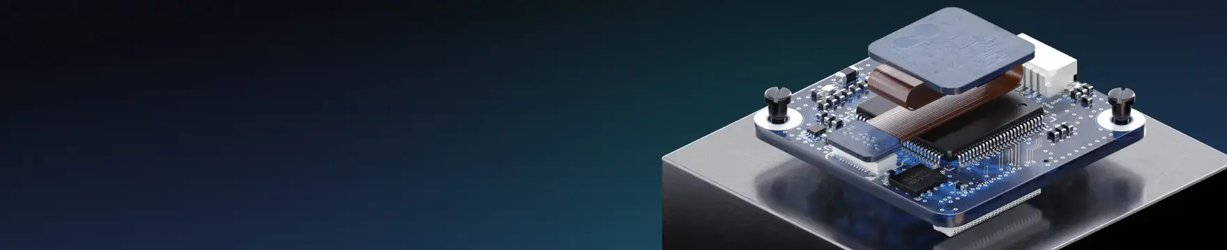
Daughter board Part 1
Setting up an Assembly Library
- Make or open a separate library for your Assembly designs, This will become a very large library very fast and you do not want it to conflict with your main library or libraries.
- After you have completed the design for the daughter board,
- Open the daughter board design and pull down the File menu from the top,
- Select the Export sub-menu and slide right, then select the Step 3D sub-menu,
- Chose the name for the daughter card assembly and put it into the File Name box, Make sure that you include the step extension and make a note of the data path.
- Click on the OK tab,
- After the script is run, click the OK tab to get out,
- Do a File, Save All from the top menu.
Daughter board Part 2A
Creating the Assembly PCB footprint
- Open up your both parts of your Assembly Library.
- Create a new footprint in the Assembly PCB Library.
- Place a pad at the X 0, Y 0, Make sure that the pad and drill are the correct size for the assembly.
- With the Properties window open, pull down the Place tab at the top.
- Slide down to the 3D Body tab and click on it.
- Click on Generic tab in the Properties tab and then click on the Choose tab in the 3D Model Type section.


Daughter board Part 2B
- Navigate to the daughter card database, select the step file and click Open,
- Rotate and position the 3D image so that the Pin 1 is positioned in the center of pin 1,
- Select the pad and copy it, then Paste it onto all of the other pins positions, If you setup the grid for the pin to pin spacing, you can set the pins faster.
- Renumber the other pins to match the connector that is on the daughter card,
- From the PCB Library menu, highlight the footprint,
- Add the an outline of the board and connector to the top silkscreen layer, The 2 outlines will help place and show where the daughter board goes.
- Right mouse click and rename the footprint to the name and description of the assembly footprint,
- Do a File, Save All from the top menu.


Daughter board Part 3
Creating the Assembly SCH symbol
- From the SCH portion of your Assembly Library,
- Either copy/paste an existing part or create a new one,
- Make sure that you have all of the required pins for the interface with the main board,
- Name the pins with the signal names that were used from the daughter board interface,
- From the PCB portion of the Assemble Library, Highlight the footprint that you will use with the new part and make a copy of its name,
- Switch back to the schematic portion of your Assembly Library,
- Double click on the part number to open the Properties menu,
- Click on the Add tab of the Footprint section,
- Either Paste in the Name of the footprint or navigate using the Browse tab to select the footprint,
- Click on the OK tab to set it and pull down the Project menu from the top,
- Click on the Compile Integrated Library,
- if problems fix them or review the parts and verify that the new part was added to the Assembly Library.
- Do a File, Save All.
Daughter board Part 4
Adding the Daughter board to the Main board
- Open the main board project file and its SCH file,
- Navigate to your Assembly Library and add the schematic symbol for the daughter board to your main design schematic,
- Do a File Save All from the top menu,
- From the top, pull down the Project menu and click on the Compile PCB Project,
- From the top, pull down the Design menu and click on the Update PCB Document,
- Select the desired Component Links,
- Click on the Perform Update tab and click Ok,
- Validate Changes and Execute Changes and click Close,
- Position the daughter board where you want it.
Daughter board Part 5
Running a 3D DRC between the main PCB and any daughter cards
- Place the daughter board in the position on the main board,
- Setup your Main board Design Rules for the Placement Component Clearance spacing, This gives you the 3D clearance between the Daughter and the Main board.
- From the top menu, select the Tools and pull down the Reset Error Markers,
- Now from the top menu, run the Tools Design Rule Check and click on Run Design Rule Check,
- Look and repair any conflicts that you find,
- Do a File, Save All.
Key take-aways, Running 3D DRCs
- You can add and use hidden parameters in your library parts to help filter BOMs.
- You can hide or keep parameters hidden in your schematics to help explain which parts are or are not to be used.
- The hidden parameter Unfitted is compatible with the Variants Sub-routine.
- You can do copy/paste and rename in the schematic part of the library.
- You can use Tools, Parameter Manager to globally edit and update the SCH library.
- Due to the use of mixed technologies, few BOMs can be used for everything.
- You may need 1 BOM for the assembly of all SMT components on a PCBA, another for the Thru-Holed components on the same PCBA and you may need to divide, subtract or cross reference Not/Assembled (N/A) parts.
- Altium Designer can output a master BOM that can be separated into all of the BOMs talked about above.
- You can use the Excel Auto BOM Filter template to do the filtering.
- You can simply create Sub-Assemblies of daughter cards and add them into main PCB designs.
- You can run a 3D DRC to verify that there are not any conflicts between the main PCB and any daughter cards.
Related Resources
Related Technical Documentation
Table of Contents
- Topics Covered
- Why do we need to use hidden parameters in our library parts? I.E. One BOM may not rule them all.
- What are the 3 Hidden parameters?
- How can we add hidden parameters to existing libraries?
- Part 1
- Updating the rest of the library,
- Part 2
- How can hidden parameters be used in our schematics?
- When you have a part that is not to be assembled
- Generating the Master BOM
- Reviewing and Editing the Master BOM
- How can we filter BOMs that Altium outputs?
- How can we filter BOMs that Altium outputs?
- Continued
- Daughter board Part 1
- Setting up an Assembly Library
- Daughter board Part 2A
- Creating the Assembly PCB footprint
- Daughter board Part 2B
- Creating the Assembly PCB footprint continued
- Daughter board Part 3
- Creating the Assembly SCH symbol
- Daughter board Part 4
- Adding the Daughter board to the Main board
- Daughter board Part 5
- Running a 3D DRC between the main PCB and any daughter cards
- Key take-aways, Running 3D DRCs
Design to Release, Without the Friction
- Keep reviews tied to the right version
- Reduce handoff confusion and rework
- Spot sourcing and release risk earlier
- Work solo, share when needed
Get Started
Thank you, you are now subscribed to updates.