


You Design & You Manufacture: Additive Manufacturing of Complex Multilayer Circuits

At a Glance
Explore how additive manufacturing empowers designers to prototype complex multilayer PCBs in-house - faster, securely, and with complete design freedom.


We’re in an era where product life cycles are shrinking, and the demands on PCB designers are more intense than ever. The need for speed is clear, and additive manufacturing now enables rapid, in-house iteration, all in complete secrecy.
Watch Robert Even, Product Marketing Manager at Nano Dimension, present at AltiumLive. In this session, he covers:
- The technical aspects of how 3D printing works
- How additive manufacturing is migrating into the world of electronics
- What this shift means for designers
- A wide range of applications and real-world use cases
Additive manufacturing combines advanced printing and materials technologies, but its true power lies in the control it gives designers. It’s not just a tool. It’s a catalyst for innovation and a cornerstone of any Industry 4.0 strategy.
- Explore how Altium supports printed electronics and enables the integration of electrical circuits with three-dimensional mechanical parts.
Transcript
Robert Even:
Okay—imagine if you could print a multilayer PCB in just one day, for any range or type of application. Or even better, imagine printing a PCB and a connector in a single print—combining both functional and structural elements. Or printing an antenna—one that's not only structural but also fully functional. Even something like an electromagnetic coil. In other words, imagine starting to print mechatronic designs. All of this is possible in just one day with Nano Dimension and the DragonFly printer.
This presentation is intended for both designers and manufacturers. Our goal is to open up new possibilities in additive manufacturing of complex multilayer circuits.
My name is Robert Evan, and I'm the Product Marketing Manager at Nano Dimension, a company based in Israel. We have around 100 employees—two-thirds of whom are engineers and scientists.
As you’ll see from my presentation, we're a highly multidisciplinary company. We combine expertise in mechanics, electronics, software, chemistry, and physics to bring everything together.
So, you’ve all heard about 3D printing. The 3D printing revolution has already taken place in the world of mechanics.
Fifteen or twenty years ago, a mechanical engineer would create a design using CAD software and then go through the tedious process of prototyping using subtractive manufacturing—taking a block of metal or plastic, machining it down, or creating a mold using conventional techniques. They’d have to wait a long time, only to discover a mistake, go through multiple iterations, and waste a lot of time and resources.
Then came 3D printing—first with plastics, later with metals, and eventually with many other materials. Today, mechanical engineers can produce their first prototypes much faster and more efficiently.
This technology has been around for 15–20 years. Personally, I was working at a 3D printing company 15 years ago—what is now Stratasys—helping to launch a new product to market. Fast forward to today, and we’re seeing rapid manufacturing of real-world items using 3D printing: airplane parts, components for all kinds of applications, and functional objects made from metals, plastics, and more.
What about you—the electronic engineers of today? You design your board, lay it out, and then send it off for manufacturing—a long process. Sure, it’s getting a bit faster for very simple boards, but when it comes to more complex, multilayer boards, the process is still slow and intricate.
A single multilayer board can involve over a hundred individual steps—from building up internal layers to plating, drilling, and more.
Nano Dimension is bringing the same 3D printing revolution that transformed mechanical engineering into the world of electronics.
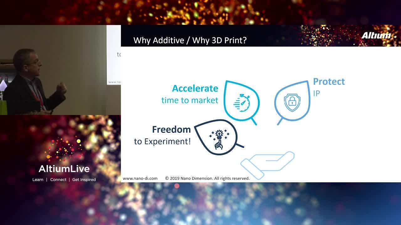
So why 3D printing? What are the benefits, and why do we want to move in this direction?
The first key benefit is that it opens up the ability to experiment. With a 3D printer in-house, you no longer need to outsource and wait days—or even weeks—for your board. In-house manufacturing means you can iterate freely and test ideas on the spot. You can try, fail, adjust, and try again—quickly and efficiently.
You have a new concept—an innovative idea—but your boss won’t approve it because there’s no time, and the schedule is tight.
Having a 3D printer in-house gives you the freedom to experiment. This shift has already happened in mechanical engineering, and now it needs to happen in the world of electronics as well.
With in-house 3D printing, your first iterations can move much faster, enabling you to reach the market sooner. You’re able to work agile, iterate quickly, and progress in parallel, rather than waiting for each round of outsourced prototyping. This accelerates time to market significantly.
Another key advantage is IP protection. Many companies—especially in defense and high-tech consumer electronics—are concerned about sending their designs out during early development stages. With 3D printing from Nano Dimension, along with other technologies I’ll touch on, you can keep your designs in-house longer, which provides added security and value, particularly in sensitive industries.
And finally, it’s a much more resource-efficient process. There’s no solvent-based manufacturing, no unnecessary waste, no excess PCBs, and no shipping involved. It’s all done through additive manufacturing—you produce exactly what you need, no more, no less. It’s extremely efficient.
Now, because of all this development, it's important to understand the difference between printed electronics and 3D printed electronics.
Printed electronics—as demonstrated by TactoTek this morning and a few other companies—typically involves screen printing a single layer of conductive material onto various substrates. This is often used to make flexible antennas and other functional components.
The IPC has been following this space closely and has already established standards covering design guidelines, functional requirements, base materials, and newer documentation addressing application categories and design terminology.
But now, let’s talk about the next stage: 3D-printed electronics. This is a newer area with exciting potential. There's a protocol—IPC 7991—and an active committee working on it. Our own product manager is part of this committee, along with members from companies like Optomec, who also have solutions in this space.
This committee is focused on defining process guidelines specifically for 3D printed electronics. You saw a glimpse of that in the presentation by TactoTek this morning.
Now, I’d like to walk you through what’s currently out there in the world of 3D printed electronics—and how Nano Dimension fits into that picture.
So first, there are players today offering basic desktop solutions that are inexpensive yet effective. These allow you to create a two-layer board with around 200–250 micron trace widths. While the material may not be highly conductive, you can still build simple boards that support soldering and paste application. It’s a great low-cost, quick-and-dirty option for basic two-sided PCBs.
In addition, there are consortiums and collaborative groups of companies combining different technologies to explore new approaches in 3D printed electronics.
One example is a Dutch organization called TNO, which is working with SLA 3D printing and metal deposition technologies. There’s also Nix Factory, which was particularly active a few years ago—bringing together four different technologies in a consortium-like setup to offer a 3D printed electronics solution. Another example is CDR, a company with an excellent inkjet printer. They collaborate with third parties, selling their printers to companies that develop specialized inks and processes.
All of these are very good solutions. They’re excellent lab tools and provide a strong foundation—but they’re not truly commercial-scale solutions.
Where we start to see commercial solutions is with some of what you saw today. For example, TactoTek offers excellent commercial capabilities. Optomec uses aerosol jetting—they take nanoparticles, convert them into a gas, and precisely deposit them through a fine nozzle. This allows them to print highly conductive materials onto complex surfaces, sometimes using CNC support.
Other notable technologies include MesoScribe, InScribe, and again, TactoTek, who presented this morning. There's also LDS technology from LPKF, a German company known for their PCB milling machines. They’ve developed a process using injection molding and plastics, where specific areas are laser-treated and then metal-plated. This enables 3D contours with metal features—an impressive combination of mechanical and electrical integration.
All of these are excellent commercial solutions, well-suited for production. They offer reliable single-layer deposition on a wide variety of surfaces and contours.
Now let’s take a look at what Nano Dimension offers—because what we do is something different.
What you saw in the video is that we’re taking a completely different approach. Nano Dimension is building multilayer PCBs using a 3D printing methodology, similar to what we discussed earlier in the context of mechanical engineering. We're applying that same layer-by-layer approach to electronics—constructing a multilayer PCB (an assembled PCB, or PCBA) entirely from scratch.
In a single process, we build up both the dielectric material and the conductive layers—simultaneously and precisely. I’ll go deeper into the technology shortly, but what this enables is truly transformative for your workflow. It allows you to innovate faster, test multiple ideas quickly and affordably, and remove many of the traditional barriers to experimentation.
There’s no need for internal PO bureaucracy, no outsourcing delays, and no shipping time—because the printer is in-house. There’s no minimum order quantity, and no reason to hesitate when you want to try out a new concept.
Again, innovation is what we’re really aiming to enable.
Here’s how it works in the Nano Dimension DragonFly ecosystem: You design your Gerber and Excellon files just as you do today—no change to your existing workflow. We’ve developed software that imports those files seamlessly.
In a setup process that takes just 10 to 20 minutes, you define the Gerber file layers, ensure the Excellon data is properly registered to your routing, and then send the job to print. From there, the system begins depositing thousands of layers, building your board from the ground up.
By the next day, your board is ready—ready to be soldered and tested. It’s essentially one-day PCB printing, using the same design files you already work with today.
So what can you do with it? You can create functional antennas, sensors, and more. Over the past year, we’ve seen this first-hand through our customers. We’ve deployed about 30 printers worldwide, and as more users adopt the technology, we continue to discover new and exciting applications every day.
In the field of antennas, for example, we're finding that our results are very close to those of traditional materials.
When it comes to sensors, many users are already leveraging our printer to create them. You can produce high-quality proof-of-concept models—take an idea and validate your design by the next day.
You can build prototypes, test fixtures, and custom adapters quickly. For example, the fixture you see here was printed in about three hours. If you encounter an error in your design, you can fix it right away—rapid iteration is a huge advantage with a printer like this.
Another great example is what our German partner, Phytec—a system-on-module (SoM) manufacturer based in Mainz—was able to achieve. They loved our technology and purchased both our beta printer and commercial printer, and are now also working with our distributor.
What they did was impressive: they 3D printed the plastic housing, 3D printed the board, and were able to show their customer a fully functional prototype within just one day.
That’s the power of 3D printing and additive manufacturing.
Here’s another great example of how they used the technology. Since Phytec operates in the electronics field, they were able to perform rework very quickly thanks to the DragonFly printer. Phytec had a job to deliver 24 prototypes of a board to their customer. Just two days before the deadline, they discovered an error in one of the schematics. What could they do?
They initially estimated that the rework would take two to five weeks. However, because they had access to the DragonFly printer, they found a much faster solution. The issue was related to a simple component—a 6-pin BGA, measuring just 4x4 mm.
In about six hours, they were able to print 30 of these components. They then soldered the corrected component onto each board. Power-up and testing took another half a day.
In total, they completed the rework in just one day, effectively closing the loop and saving the project—ensuring Phytec delivered on time to a very important customer.
And again, that’s the power of improvisation and rapid response with a printer like the DragonFly.
At Nano Dimension, we have two main lines of additive manufacturing. When we talk about additive manufacturing and where this technology is headed, we’re starting with prototyping and identifying areas that can scale into manufacturing.
Our first focus area is PCBs, RF antennas, and basic electronic devices—and that’s what we’re showcasing here. There are many examples we could share. Here’s one: a sample coupon that gives you a feel for what’s possible with our technology.
It’s a four-layer board with blind and buried vias, plated through-holes, and 100-micron trace widths—just to give you an idea of the specs. Feel free to pass it around. That’s what you can do today. But what’s even more exciting is what you’ll be able to do tomorrow—like creating fully integrated electromechanical devices.
You can print in 3D. Since we're depositing layer on layer, there's no need to stay planar—you can build three-dimensional structures. We have a sample coupon you can pass around to see what's possible.
This represents the future: creating 3D designs with embedded electronics. It’s a developing field, harder to define, but already showing potential in various applications.
Edge accuracy is critical. You can print on very fine structures. For example, if you need a one-millimeter width, the tolerance is typically around 15–20 microns. For a 100-micron feature, the result might vary between 85 and 115 microns due to pixelization, not plating. This variation remains roughly the same even at larger sizes like 500 microns.
We use inkjet technology for its precision and ability to print multiple materials. Our system uses two printheads simultaneously: one deposits a nano-silver conductive ink, the other a polymer dielectric. Together, they build the entire board from scratch, layer by layer.
Everything—the annotation, embedded annotation—we do it with silver ink embedded inside the solder mask. The solder mask is done with a dielectric ink. Signal layers are done with silver. Insulation layers are done with dielectric. Through-holes we can also do easily, and vias—we can fill vias.
Think about 3D printing. What is the advantage of 3D printing? As you understand, we’re building up layer by layer. Think about it—vias can be built up. Now, vias are not holes; vias are pillars. So, if I want to join layer two and layer three in a six-layer board, I just build up drops layer by layer between layer two and layer three.
So if I have a PCB and there is one via, or 1,000 vias, or 10,000 vias—and they’re all blind and buried vias—it’s the same amount of work for us. Very easy for us to do. The technology doesn’t care about complexity.
And so, a printed circuit board of ours would look like this: the dielectric is continuous—we’re just continuously building up the structure of the PCB. The vias are filled, there are conductors and other features throughout the board—ground layers, whatever—but it’s a continuous build.
We’ve developed software called Switch. The Switch software is supported by a large development team—about 10 software engineers. We’ve done extensive work to enable the import of Gerber files, set them up layer by layer, and generate a 3D file that can be easily printed.
We also have a strong focus on algorithm development to optimize the printing process, which is why the printer is not just laying down layers blindly—it's actually very smart. There’s a significant amount of software intelligence built into the system, tightly integrated with our process.
In addition, we’ve developed two proprietary inks. One of them is a polymer ink, which acts as the dielectric.
We call it a liquid FR4 because its material properties are very similar to standard FR4. It has a dielectric constant of 2.9 at 1 GHz and a loss tangent of 0.02.
What’s really exciting is that we’ve tested this material—both internally and through third-party labs—and found that when operating at 5, 10, or even 20 GHz, the material properties remain remarkably stable. This is unlike traditional materials like Rogers or FR4, which tend to vary more at higher frequencies.
This material behaves differently—it stays consistent—and that’s something we’ve only come to fully understand in recent months. External testing has been confirmed by our own internal validation, and we’re very excited about the potential this offers for high-frequency design applications.
This dielectric ink has been specifically optimized for 3D printing and is fully compatible with our conductive ink.
Here’s how it works: the dielectric material starts as a liquid monomer—before it becomes polymerized. It is inkjetted onto the surface, where it spreads slightly, and is then immediately cured under a UV lamp, which hardens it. This forms both the dielectric layers and the 3D structure of the printed object.
All of this happens on the fly, layer by layer, at micron-scale thicknesses. As mentioned earlier, this same dielectric material is also used for the solder mask.
Question:
How thick would the polymer layers between the conductive layers be, at minimum?
Robert Even:
We do have a minimum layer thickness, and I’ll cover that in more detail in a few slides. But to give you a preview—our spec allows for 10-micron layers. So, you can create 10-micron dielectric (prepreg) layers, 10-micron silver layers, and anything above that.
You're not limited by traditional standards like one-third ounce, half-ounce, or one-ounce copper. You can print whatever thickness you need—15, 20, 30 microns—whatever suits your design.
The silver ink we’ve developed is a nano-silver ink. It's a liquid ink we formulated in a solvent, with silver nanoparticles suspended in it. When printed, the ink is jetted onto a heated surface using an inkjet head. The solvent evaporates, leaving behind the nanoparticles.
These silver nanoparticles are then immediately passed under an infrared heat source, which sinters them—making them conductive.
All of this happens automatically, layer by layer, with micron-scale precision. You don’t have to intervene—everything is handled by the system in real time. As for the spec, you can build boards up to 18 x 18 centimeters. Thickness can range from 0.7 mm and above.
If you go below that and beyond our design rules, well—oops—it ends up flexible. And you probably don’t want that, do you?
It’s flexible, but it’s not true flex—I’ll talk more about that later on.
The minimum layer thickness for both the dielectric and conductive materials is 10 microns, and you can go with anything above that.
Your line/space resolution is around 100 to 125 microns. Here’s a look at what that looks like under a microscope—you can see silver features and 125-micron spacing.
This is also what it looks like across various PCBs we've produced. We’ve done over a hundred benchmarks for companies around the world, and this gives you a sense of what some of the features look like.
So, here’s a bit about the setup I mentioned earlier. Again, using standard Gerber and Excellon files, it’s a very simple import process. The layers are laid out, and you just define each one, layer by layer.
What’s really nice is that at the bottom here, for each layer, you define: top layer, number one, number two, number three, etc. And for each layer type, you define the order and the thickness. So you can start playing around and do all sorts of innovative testing.
If you want 10-micron layers here, 20-micron layers there, or maybe you want to compensate and print 80-micron layers, you can play around and do anything—layer by layer. For each one, you define the conductor; for each one, you define the prepreg. You can also experiment with different prepreg thicknesses if you wish.
Then you define the other layers—the solder mask layers, the route layer—you assign everything. You take the Excellon drill data, define the drills, and you make the vias, which can be as small as 200 microns. Plated through-holes can be down to 400 microns.
We set all the layer parameters, we set all the thicknesses, and we checked everything.
This is typically a 10 to 20-minute setup process—apply everything, make sure everything is correct, and check your thicknesses.
Here, we reset one of the thicknesses because, when we set up the whole board, we found it was too thin. So, we changed it to 1.6 millimeters, set it up on a tray, and then it’s ready—ready for printing.
Here’s another example: they found something else and changed the insulator thickness above, and the prepreg was also changed to ensure the total thickness matched the design.
This setup is done manually today—it’s not that complicated. Maybe one day we’ll automate it as part of the setup process. But that’s it—you’ve set up your job, sent it off to the printer, and it starts printing.
This is what you’ll see: after preparing your job, you can monitor the print status. For example, here we’ve printed 148 of 3,046 slices—this job will take about 15 hours, and you can watch the progress as it goes.
Basically, that’s what happens—you come back the next day, and your board is ready for soldering.
Question:
What about the ink?
Robert Even:
You don’t need to worry about the machine itself—the software tells you in advance. It knows you’ll need, say, 4 milliliters of ink. These boards require very little material. Even a larger board may only use 5 to 8 milliliters of ink.
You always check that you have enough ink before starting. If you need to replace it, it’s very simple—just a quick cartridge replacement, like with any standard 3D printer. Very easy to do.
The software will always notify you if you're low. If you have enough, you go ahead with the job. If you don’t, you’ll know ahead of time—it won’t wait until you run out.
And yes, you only need two materials: the inks.
Today, we have two materials: a silver ink and a dielectric ink, which is a polymer. In the future, we'll have other inks that can do things like support structures. If we get into 3D printing and have an overhang, you’ll need support material.
We have a very large chemistry department, and we understand that the future lies in developing new inks. Maybe we’ll find an ink formulation where the silver is even more conductive, or we’ll develop a dielectric material that’s stronger—especially if we start building 3D structures up to one centimeter high.
So, there's a lot of chemistry and ink development that we’ll be focusing on in the future.
Today, our first-generation product uses two inks: one silver, one dielectric.
You can also scale up. If we want to increase speed, inkjet printers can be expanded—I’ve worked with a company that used 150 printheads, so scalability is very achievable.
Question:
Would it survive a reflow oven?
Robert Even:
It will survive a reflow oven, but at a lower temperature. So today, if you have a big board like this, we recommend using bismuth or indium-type inks and reflowing at 140 degrees.
However, what’s nice about this printer is that it goes out to the field—and then people don’t listen to us. They do whatever they feel like—even a German company like Phytec.
So, what did Phytec do? They took a board about this size and said, “Yeah, yeah, you tell me 140, but I have vapor phase, which is more homogeneous. This board is that big—I’m going to do it at 240 degrees, standard paste.” And it worked.
What happens at higher temperatures is we get some warping. So, a large board at 240 degrees will warp. However, small boards at 240 degrees will not warp, and there’s room for us to improve that.
There’s room in material development and process development for us to close that gap.
But today, you can make small boards, and the bigger boards—they’ll warp. If not, you can use lower-temperature soldering with bismuth or indium-based inks. So, it is possible to solder these boards.
You can get a feel for one here—there’s a small working board, a very simple one, but just to give you a sense. Again, it’s slightly more fragile than traditional materials because we don’t have a mesh inside like FR4. But you can get a feel for what the board can do.
Here are some more things you can do: round boards, very complex routing—which is very easy with this printer because there’s no cutting involved. You just lay it down. If you want to start experimenting with complex routes, this is a great printer for that.
Here’s a soldered round board. Here’s a 12-layer PCB.
Sensors—we have a few sensor applications that are working very well.
And antennas—as I mentioned before, we’re seeing very good results with antennas.
Here’s a look at what soldering looks like up close.
We have done a lot of work now to provide you with guidelines. We're now sharing guidelines on soldering our boards, specifically with manual soldering and lower-temperature materials.
But again, the field tends to do whatever they want. Two days ago, I was at a German customer who said, “Yeah, we saw your low-temperature guidelines, but we used regular paste—and it worked just fine.”
So things work—people find workarounds. Once they learn the materials and see how they behave under heat, they understand what's possible.
We weren’t PCB experts initially, so we were a little too cautious. But now, we’re discovering that you can actually do more and more with our inks.
Question:
What about if you have a BGA component?
Robert Even:
A BGA component—that’s exactly why our German partner, Phytec, said, “We don’t care about your 140°C guideline. I have to melt the balls.” So they did it—and it worked, on a smaller board.
If you have a big board, there will be a problem doing a BGA. You’ll probably need a sub-board or need to reball. There are a few workarounds available today.
But you can make a smaller board and run vapor phase reflow at, for example, 240°C.
Question:
If you make a board and it warps, will it become flat again?
Robert Even:
No, it's a bit tough. Our guys have played around with it in the lab—sometimes they can, but it's not really reliable, especially if you already have components on it.
But I've also seen boards—depending on where the components are and how many components there are—that are slightly warped, and the contact is still good.
You have to look at it case by case. For a very sophisticated board, you probably can’t.
Question:
In the designs that you have shown, I have not seen PCBs with complete ground layers, for example.
Robert Even:
Yes, that would also be possible—to make complete ground layers.
I can’t really pass this one around, but you can come take a look. A lot of our boards have ground layers. We’re printing them—50% to 80% of our benchmarks even have large ground layers.
This one—you can come and see if you want afterward. It’s not a fully released board like the others, but you can pass this one around. There are some ground layers on the back.
Question:
How does the resistivity compare to traditional materials? Is it better conducting?
Robert Even:
Silver is not as good a conductor. In the lab, in pure, ideal settings, we can get to 50%. In the real world of printing on this printer, we can get between 10% and 20% conductivity today. That’s why I’m emphasizing antenna applications and sensor applications. But that is constantly improving, so I expect it to go up. I don't know by how much, but that’s where we’re at. We're at about 10 to 20%, which is common with many silvers that are not pure silver.
Question:
So you're able also to produce—when you're printing passive components?
Robert Even:
Passive components—we're not able to yet. That’s down the road. It is possible. Again, this DragonFly printer is really an R&D platform where you can do so much. There is the possibility to develop materials that will become passives—you can print passives, you can start printing conductors and create a small resistor if you want. There are a lot of possibilities. As the technology matures, we’ll get more and more into that. I’ll show you at the end a little bit of our proofs of concept for some future developments. That’s something that’s really further down the road, but it is possible with this technology.
Question:
Potentially, you can also do different areas of different layers—that can happen, right?
Robert Even:
Different areas?
Question:
In the same PCB, with different layers—that can happen?
Robert Even:
Yes, yes. You would probably have to combine them at the Gerber file level. The current system doesn’t support it, but potentially, you could. Yes, for sure. Because we’re starting from basic micron-sized layers, so you can play around.
Question:
Can you bury the component into it?
Robert Even:
You stole my second-to-last slide! We’ve done a proof of concept on that—I’ll show you.
Okay, so let’s continue. So, what can you do? What application areas can you explore?
If you look at the right-hand side, in all these areas—defense, automotive, research, aerospace, consumer, medical, IoT—what stands out is: We’re very good at antennas, we’ve learned we’re very good at sensors, and we can open up non-planar designs like nobody else can, because we can do everything from scratch. You can also do rapid prototyping in almost all of these areas.
In research, you can create advanced functional prototypes, and in consumer and IoT as well. You can save weight, you can make smart parts—there’s a lot that can be done with this technology.
You need to apply and adapt it, and unlike many other technologies, we give you the printer, and you can start doing things we never even told you to do. You can begin conducting your own R&D, and many of the companies we’ve sold to—innovation groups—are developing things we have no idea about.
But that’s the idea. This is actually democratizing design, because you can start experimenting and doing things we never even imagined—just by having the tool in-house.
Question:
Can you import a STEP file or something similar?
Robert Even:
What we've done is we've worked with SolidWorks very closely. You’ll see that in one of the last slides, where we show how we can take a STEP file and 3D print it.
In SolidWorks, you define two materials—conductive and dielectric—and we can print today up to three millimeters. There’s an add-in that SolidWorks has developed to allow you to do this seamlessly.
That’s how we printed this 3D coupon that’s going around—using a STEP-like file or a SolidWorks file.
This is a little bit of what it looks like on the inside. This is already from six months ago, so I’d say we’re even better today.
You can see everyone sending us these annoying daisy chains of conductor–via–conductor–via—sometimes a hundred of them—to test how good our connectivity is.
Here, you get an idea: the conductor goes slightly up against the via, but we’ve passed a lot of that testing. And this is a bit of what it looks like on the inside.
What we've seen—I talked about antennas—where is this based? It's based on work we've done with Harris Electronics in the United States, a leading military electronics company. They gave us an RF amplifier design, we soldered components, they tested it, and said, "Guys, you are roughly at the same level as FR4 and coaxial connectors."
Why? They tested it at 4.7 GHz and found about a 1 dB gain difference, and at 6 GHz, there was less than a 1.3 dB gain difference.
Next week, at an IEEE conference in Florida, they’ll be making two presentations discussing this breakthrough—printing antennas and RF amplifiers with our materials.
It's not too surprising, because there are already a lot of silver antennas out there. If you're involved in printed electronics, you’ve probably seen them—they perform quite well.
So, this is a major advantage of our technology, and that’s why we’re pushing hard to explore more antenna applications in the field.
Also, sensors—again, this was done by Phytec, our partner in Germany. They didn’t care—it was 18 x 18 millimeters, and they vapor-phased it at 240°C because it had a BGA.
It worked on a smaller board and resulted in a very nice temperature and humidity sensor that they used in one of their applications.
Now, this is a new technology we launched a little over a year ago. We've achieved the basics, and now we're moving into areas like controlled impedance and signal integrity.
You can see on the right—we're starting some early testing, and we’ll see where we end up in that field.
RF performance—we talked a bit about that. We recently discovered that at 20 GHz, the material is performing quite well—very similar to 1 GHz. There's real potential there for high-speed circuits.
Power circuits—we’ll have to see how we manage those, since we’re not as conductive.
Reliability and longevity—we recently received a report from a major manufacturer. We passed 2,000 hours at 90°C, with only about a 3% change in resistivity. They also did temperature cycling from -40°C to +85°C, across 200 cycles, and we passed that as well.
I was honestly very surprised, because in principle, these materials aren’t considered highly durable—but they passed these tests.
We have the results from this company, and what’s most interesting—and getting a lot of buzz—is the EDA and CAD worlds coming together.
There was a presentation earlier today, and the best example is how Altium and SolidWorks are working together right now. As I mentioned, we work with SolidWorks, and Altium is working toward enabling a future where you can have an eight-layer board with complex contours, and print it using our printer.
We’re essentially providing the infrastructure the industry needs to make this possible.
If it happens at the design level but no one can actually implement it, progress will be slowed. That’s why we’re offering this infrastructure—to help move the industry forward.
And then let's talk about the 3D aspect. Here's what we do in SolidWorks: you define two materials for this coil—conductive and dielectric. Today, it's really planar, but with our technology, tomorrow it can be spiral. SolidWorks has an add-in that allows you to seamlessly pass the design to our printer and print it. Together with Altium’s ongoing work, this collaboration will make it all happen.
On the right, you can see the result. What we did was actually print these coils, and a lot of people are interested in coils because of the magnetic properties they offer and their applications in various fields.
So, we printed that using SolidWorks. You’ll notice it’s a bit thicker than a typical PCB. This example uses two layers, but it can be expanded to more. As I mentioned, it can be spiraled—we're still exploring and learning the design possibilities.
You can see that it works well as an electromagnet. If you print it thin, you can even make it flexible.
How flexible? Well, it’s not Kapton, but it opens up the possibilities. We know it’s possible to develop polymers that are Kapton-like, and we can also develop flexible silver. With that, we’ll have a real path to achieving flex-rigid boards in just one day. That’s the future.
And this is the embedding someone mentioned earlier. What we did—using the SolidWorks setup I talked about—is we printed a 3D file with a cavity. We stopped the printing mid-process, the tray came out, we manually placed in two resistors and two LEDs, then sent it back to print.
It continued printing on top—the conductor connected to the contacts, and then we covered it with dielectric. So what we had was two embedded resistors and two embedded LEDs, protected and completed as a proof of concept.
That means it was just a first attempt—not yet a fully reliable process. We're now working on turning that into a repeatable, production-ready method.
Once we do that, it opens the possibility of creating a complete object. That’s why, if you think about the future, 3D printing could one day allow you to print different materials, embed components, and build the electronics inside—resulting in a fully functional remote control or other complex object.
So, in summary, when we talk about Industry 4.0 and IoT, what we really need is the endless possibilities of 3D-printed electronics.
There are many technologies out there, but we have adopted a kind of holistic approach—building everything from scratch—to open up the real possibilities of 3D printing across the entire platform, where you get all the benefits that 3D printing has to offer.
We talked about mechanical engineers at the beginning—fast prototypes, a lot of innovation.
Today, we can do complex multilayer PCBs and functional antennas. And tomorrow brings even more possibilities—embedding in 3D, and beyond.
It’s all out there, and this is the platform to do it.
Thank you.
About Author
Related Resources
Related Technical Documentation
Design to Release, Without the Friction
- Keep reviews tied to the right version
- Reduce handoff confusion and rework
- Spot sourcing and release risk earlier
- Work solo, share when needed
Get Started
Thank you, you are now subscribed to updates.

