The Ins And Outs Of Receiving And Inspecting Manufactured PCBs


When it comes to the process of receiving and inspecting manufactured PCBs, there are two dominating factors: Specify as much as you can on the fab drawings you provide to the PCB manufacture, and thoroughly inspect your first builds to ensure that all of those specifications have been satisfied and that no errors have crept into the fabrication process.
This article provides an overview of the receiving and inspection process; the things that need to be specified; the “hidden gotchas” that can be lurking at every turn and how to create fabrication notes to ensure that the board you designed is the board you receive. As with other efforts, I worked with John Zasio our partner in Speeding Edge who has very recently gone through the receiving and inspecting of bare board PCBs for a variety of his client efforts.
The Devil Is in The Details
Delving into receiving and inspecting procedures, there are a few basic premises to keep in mind:
- Don’t assume that your fabricator will be able to “guesstimate” your board specifications. As these elements are design-dependent, specify the critical factors that will make your board a go/no go proposition. Be as precise as necessary and don’t leave critical elements to chance.
- The higher speed your board is, the more critical it becomes to get these details nailed down. There is a lot less fabrication “latitude” with high-speed boards.
- It’s better to find errors on a first build board than it is on one that is populated with components that can be the equivalent of hundreds of thousands of dollars.
- Keep in mind that having to restock components can be both a costly and lengthy process that can compromise overall product quality, profit margins, and critical time-to-market windows.
Verifying the Mechanical Specifications
John explains, “There are two phases to incoming inspection. The first and most thorough is the first build. That’s the point where the fab house has to list all the drill sizes and the outer dimensions of the boards, document the laminate material used, and get all the pads and the mechanical dimensions right.”
“First, I start with a checklist comprised of the following mechanical measurements:
- The outside dimensions of the board.
- The board thickness on at least four corners, the center, and the four sides.
- In terms of board thickness, I have gotten boards that were way off on one side or the other.
- Where there are multiple boards in the panel, some of the boards can be very thin while others will be very thick.
- This means that the fabricator has introduced an error into the lamination process.
- If the board varies in thickness, from one side to the other, it changes the impedance of the transmission lines.
- This is not just a matter of taking the mechanical dimensions and making sure they fit in the box.”
“The next thing I do is check all the finished holes to make sure the fabricator picked the right drill size,” he continues. “A lot of designers will make a drill table on the fab drawing. They just put down the finished hole size and leave it up to the PCB fabrication facility to pick out what drill size they want to use.”
“I have found that the foregoing steps, especially for high-speed boards, are not enough. For the critical holes, I specify the actual drill size I want because that will determine the mechanical strength of the small holes. It also determines the impedance of the via when we try to make them like high-speed transmission lines. If a hole is drilled at the wrong size, it’s basically like taking a piece of coax and changing the center conductor diameter which changes the impedance.”
Following the foregoing, the next step is to check all the pad sizes to make sure that the pads, specifically for the BGAs, are of the correct dimensions and that an adequate solder mask is being used. It should be noted that it’s very important to check the holes for the press-fit pins very thoroughly, not only on first builds but on all subsequent builds.
John states, “If these holes are off by just a couple of mils, either the press fit won’t go in or it ends up being very loose.”
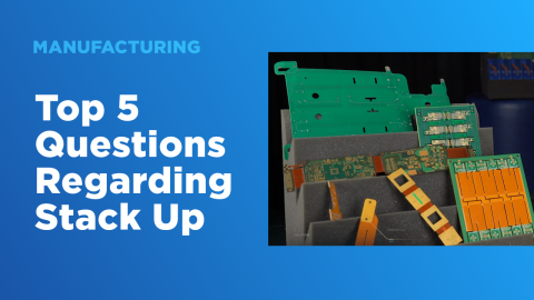
At Speeding Edge, we put a stackup coupon right on the edge of every board that we have built. It’s important to have these coupons on every board from the first build-up through final production so that a sample of boards can be pulled and examined to validate the foregoing mechanical specifications.
The Electrical Specifications
John states, “There are several things I do in terms of electrical measurements. One simple thing I do is to measure the capacitance on each power plane. This reassures me that the fabricator is using the right laminate and that the various plane and ground layers have been stacked in the right order.”
The next critical step, in terms of electrical performance, is to check the transmission lines. John notes, “This is the area where I have a lot of problems. For example, the fabricator will provide you with a report not only on the transmission lines but they will also give you a report on the impedance measurement on every level. The problem often is that they do this validation on their test coupon. This test coupon may not have the same characteristics as your board. And, their test coupon may not be etched or laid out in the same manner as your board. This is why I put my own test coupon into every board I have built.”
He continues, “Years ago, I worked with a company that would manufacture their test coupons with solid copper on both sides of the transmission line, 20 mils away. This enabled them to get a very even 50-0hm transmission line. But that’s not at all like what I had on my board. I had thieving patterns that were 100 mils away so they were spread out.”
“This is part of the reason why I have test coupons built directly into my boards. I don’t care what the etching is on the fabricator’s test coupon. It can be very different from what is on my board and that’s what I care about—what’s the impedance on my board.”
John adds, “If the impedance is way off it can be due to a number of things—the wrong laminate, the wrong thickness or over-etching. It’s easy to measure the DC resistance of the line by using a simple ohmmeter. It’s accurate enough to determine whether or not the transmission line is the proper width.”
“The latest issue we have to contend with is frequency versus loss. This is critical when you have high-speed designs with 10 and higher Gb/S lines. At these speeds, the frequency versus the loss of the laminate becomes a very crucial factor. Sometimes, the fabricator doesn’t use the specified laminate or they pick a different glass weave than that which is specified. Although the replacement weave may have the same thickness as the one specified, it can make the boards and the components on them unusable. And while you might be able to readily obtain the correctly fabricated boards, the components can be another issue [as noted above].”
The foregoing is the primary reason for doing the incoming inspection. Product developers need to know that the boards they receive are good enough to work before the board is populated with all of the components. John explains, “If you have a bunch of bad boards the last thing you want to do is to use up all your components, not be able to get more in a timely manner, and not be able to ship your product.”
Truths, Half-Truths and Downright Lies
In an ideal world, we all like to think that the suppliers with whom we do business hold themselves to a high level of ethics. But, as often is the case, the reality can be a different matter altogether.
John notes, “Unfortunately on boards that do not meet specifications, 50% of the time, the people inspecting the board and supposedly running the test at the vendor just lie about data that’s on the report they give you.”
“If you reject a batch of boards because of an obvious thing that the fabricator has lied about, such as the impedance being off by 20% on one layer of a 25 Gb/S board, they will say ‘We don’t know how that could have possibly gotten off by that much. It wasn’t that way on our test coupon.’”
As stated earlier in this article, the test coupon provided by the fabricator may be completely different than the test coupon specified by the customer. John continues, “If you check the boards you get from the fabricator and reject a batch of them, the fabricators will put a check by your name and say ‘These people have enough smarts to check their own test coupons, so we better be right.’ If you don’t check the test coupons from the fabricator, they will just ship crap.”
What Documents Do You Need to Provide to the Fabricator?
As can be readily understood, the time and effort put into creating the documents that you send to the fabricator should correlate with the quality of the boards you receive. For his boards, John says, “On your fab notes you typically list the kind of things that you want tested. On impedance-controlled transmission lines, you provide the list of the impedances. Then, based on this information, the fabricator will build a test coupon and give you an impedance test report based on those test coupons. In that same document, there are several mechanical measurements very similar to the ones that I cited earlier--board thickness, plated through-hole sizes and mechanical dimensions.”
He continues, “The fabricator has a whole list of stuff that they provide to you in a report. Supposedly, all that info has been checked. In every one of the cases where I have had problems, I found something wrong with the information that was within that report. The fabricator’s numbers can be well within the limits and then there will be one set where the results are off by a significant factor. And that’s all it takes especially for high-speed boards. That one set of numbers can be the determining factor for rejecting a whole batch of boards.”
“In one instance, there was a board that was way off in thickness in terms of one side versus the other. I called the fabricator out on that and they sent me a report that said they were getting new equipment that would measure things more accurately so this would not happen in the future. I told them, ‘Don’t go buy new equipment, you have enough equipment. You wrote down on the inspection report, it’s 110 mils +/- 10 mils and this board is 120 mils thick and it was checked ‘ok.’ Read your own limits and reject the board. It’s just not within spec.”
John continues, “The kinds of things I have seen are differences in thicknesses which affect the impedance. I have seen a lot of instances where one layer was way off in impedance. In almost all cases it has been etching related. The etching should have been measured with a DC ohmmeter before the board was laminated. The boards are supposed to go through an optical scan on each internal layer to make sure the dimensions are correct and all the lines are there before they waste the effort to build the board.”
Other issues that John has encountered include the following:
- “When the vendor puts together the drill table, they have specified a drill that is too small for a real thick board. In one case, I actually specified the drill size but it was a board where we used a capped via and I couldn’t measure the finished hole size. The fabricator drilled 8-mil holes on a 100-mil thick board. The plating can’t get down into that thin of a hole. The plating in the center of the hole was very thin and it was under a 100-watt BGA. During operation, when the board expanded as a result of heating, it would pull the vias apart. So, we would get open circuits when the board was hot and when the board cooled back down, we were ok.”
In addition to the foregoing making the board inoperable, the time and money required to track down the source of the problem can be substantial and impact time-to-market schedules as well as profit margins on the product.
John continues,
- “I have had occasions where even measuring a few holes on the board isn’t good enough. Sometimes a drill will get damaged in press-fit holes. The first QSFPs will be drilled with the right dimension holes and then the rest of the board will have holes that are 5 mils oversize. In the built board, this results in connector pins that are loose. This type of problem can be a challenge because it’s only one or two boards out of a batch that are flawed. Obviously, you can’t inspect 100% of the boards, but you do have to look at a couple of boards out of each batch to make sure that the selected drill size is correct. The caveat here is that typically when things go bad, it goes bad on all the boards. If an impedance is off on one layer it will be off on all the boards because one of the layers on all the boards has been etched wrong.”
If the laminate selected for a board is wrong, it will be wrong on all the boards.
- “I really stress to my clients to make sure to check at least a few boards on every lot that comes in and make sure they put test features on the boards so the measurements reflect what is happening on the interior of their boards and not on the test coupons provided by the fabricator.”
At Speeding Edge, we have the fabricator's ship test coupons on every board as part of the build requirements that we specify. We continue to do that on high-performance boards to ensure that there is a correlation between their test coupons and ours. In one instance, we did an on-site factory visit and when we inquired about test coupons, the manager walked over to a side cupboard and said, “I just grab a few of these and put them in every group of board I build.” True, he had test coupons but they were completely independent of the boards that were being manufactured.
How Big is the Problem?
John notes that 90% of the time at receiving and inspection, the boards coming in are built correctly, and in 10% there are problems. While not a big number, that 10% can cause an entire lot of fabricated boards to be scrapped, and that in turn, as noted above, can create a variety of issues in terms of troubleshooting man-hours and dollars as well as product delivery time and profit margins.
And, if you move from one fabricator to another, you have to start at square one. As John points out, “Each fabricator makes their own drill size chart of what drill size they are going to use. And, they make their own outline drawings, and determine the routing for outside of the board.”
For a point in time, the percentage of problems was greater for those boards that were manufactured offshore. John notes, “A lot of customers are sending their boards off-shore in particular for volume builds. As a result, the capabilities of the off-shore fabricators have come up exponentially. It’s taken them a while to get educated on high-speed boards but they are doing pretty well now.”
He continues, “A lot of companies are having large volumes of boards that run from a few kilohertz to a few megahertz built offshore. These types of boards run at low power and they don’t have the electronic requirements that you would have in 5 Gb/S boards.”
0.John expands on the foregoing by stating “It’s the high-speed boards that create the most challenges. The big issue is that PCB supplier vendors know how to make things that stick together. They are chemists and mechanical engineers. They are not electrical engineers. They don’t really understand what a transmission line is even though they may have purchased a TDR that measures the impedance. For a number of years, most of the fabricators were using a TDR that would average the impedance down the length of the line. So, if the wrong glass weave was chosen, the impedance changed +/- 10%, every couple of inches down the line and it would be ok if averaged. When you are dealing with Gb/S and higher boards, each one of those variations lops off 20% of the signal, so there’s nothing left.”
He concludes, “Some vendors will now do a loss vs frequency measurement but only when the customer supplies them with the equipment and the know-how to make the measurement. Even with the right equipment and know-how, very few fabricators will do this and they shouldn’t be expected to do so. They don’t have the required expertise.”
Summary
Even though incoming PCB receiving and inspection may be thought of as the end of the line operation, it is still a critical part of the overall design process. The types and detailed level of information that will be provided to the fabricator needs to be addressed from the onset of every new PCB development effort. This creates a win/win situation for the product developer as well as for the fabricator, in which the designed and as-built PCB performs as intended and as specified from the first build all the way through the end-of-life of the product.
If you want to know more, why not browse our product page for a more in-depth feature description or call an expert at Altium.
About Author
Related Resources


Related Technical Documentation

Thank you, you are now subscribed to updates.

