

Migration Guide Cadence OrCAD Schematic and PCB to Altium Designer Develop


Making a Smooth Transition from OrCAD Capture to Altium Designer Develop
In this guide, we’ll focus on importing OrCAD Capture designs. Please refer to specific guides if you need to migrate other files.
Legacy Translation
Before You Begin
This guide will show you how to import data from your legacy system into Altium Designer Develop. Before importing all of your legacy data, it’s important to ask yourself, “why do I need to import my legacy data?” Below are some of the most common considerations to consider when deciding whether to import legacy data into Altium Designer Develop.
"We have 20 years of data, and I don’t want to leave it behind.
- Does the legacy data include critical information for creating robust designs within Altium?
- Is it easier to start new designs rather than re-work the imported data to make it usable?
"Our service bureau doesn’t use Altium, but they can import Altium data. Our Altium system can import their data. Is this a reliable way to pass designs between our companies?.
- How do you maintain library integrity?
- Who has design authority?
- How do you plan to verify the data?
"We have some ‘golden’ designs that we need to bring into Altium Designer Develop so that we can up-issue them.
- How do you plan to verify the imported data?
- How much re-work is going to be needed after importing?
- You need to take advantage of additional Altium Designer Develop features once the data is imported?
"We have a library of trusted parts which we’d like to bring into Altium.
- Are there any exotic parts that you may have trouble representing within Altium?
- Do you need to add Altium-specific features (like 3D models) for every part?
- How much redundancy, duplication, and error is present in your library?
After reviewing these considerations, read on to learn how to import your legacy data into Altium Designer Develop.
Preparing to Migrate Your Legacy Data
There are four phases to migrating legacy data.
1. Prepare original data
|
2. Export data
|
3. Import data
|
4. Post import
|
Phase 1: Prepare Original Data
It is prudent to clean up your design before attempting to export. Below is a checklist of data cleanup best practices to help you as you prepare your data:
Schematic considerations:
-
Individual pin connectors (example: Block connectors) in KiCad must be modified at the KiCad tool level before migration. Alternatively, you can replace pin connectors in Altium Designer Develop post-migration.
-
Connectors should be represented as one-gate-per- pin with over 256 “gates.”
-
Ambiguous connectivity for reuse blocks must be broken apart in KiCad.
-
Remove hidden pins or implicit connections.
-
Local net names placed at wire intersection must be placed at correct locations (away from intersection point)
-
Are schematic symbols mapped to correct PCB footprints?
-
Schematic and PCB are in sync?
Library considerations:
- Do the schematic symbols match with PCB footprints?
- Does the library contain correct supply chain information and BoM parameters?
- Does 3D information need to be imported? If yes, then the height attribute should be assigned in OrCAD Capture.
Phase 2: Save Data in a Suitable Format
Supported Version and File Format
The following table shows Capture PCB Design Formats and versions that can migrate into Altium Designer Develop. This list is updated regularly, so please check with us before starting a new migration. Refer to this link for updated information.
| TYPE | SYSTEM | VERSION | FORMAT |
| Schematic | OrCAD Capture | 17.4 | ASCII (.dsn) |
| Schematic Library | OrCAD CIS | 17.4 | ASCII (.olb) |
| Legacy PCB | OrCAD Layout | V9.2.3 | ASCII (.max) |
The following file types are supported:
- OrCAD Capture (*.DSN) files
- OrCAD Schematic Library (*.OLB) files
- OrCAD Layout (*.MAX) files
Phase 3: Import Data into Altium Designer Develop
Using the Import Wizard for OrCAD Files
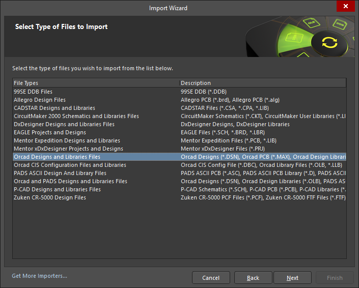
Launch the Import Wizard from the Altium Designer Develop File menu. Choose the OrCAD Designs and Libraries Files option, as shown below. On the “Importing OrCAD Designs” screen, click the Add button to choose OrCAD design files. You can translate multiple files at the same time. Step-by-step instructions on using the Import Wizard are to follow.
Starting the Import Wizard for OrCAD files
Step-by-Step Import Instructions on Importing an OrCAD Design file (.DSN)
- Start the Import Wizard with File » Import Wizard

- Select Type of Files to Import—>OrCAD Designs and Libraries Files.

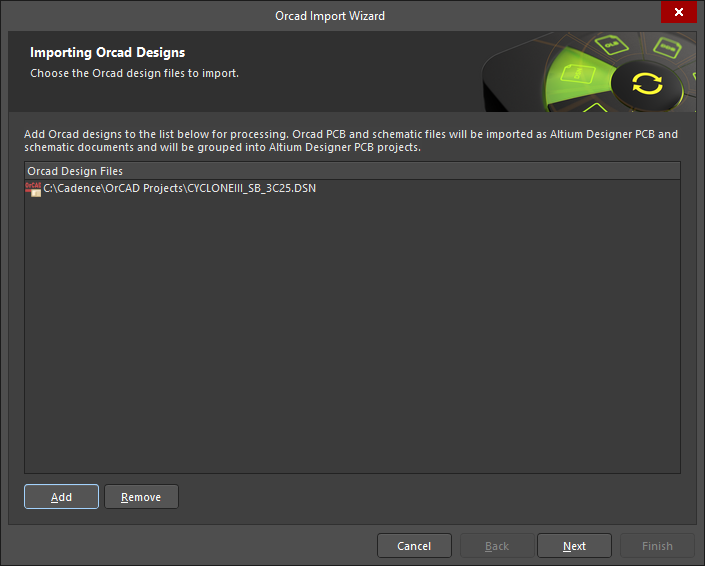
- Add the file(s) to be translated. In this case, the “CYCLONEIII_SB_3C25.DSN” file has been used.
NOTE:
You can add as many OrCAD Design files as you like at this point. However, if you add files of a
different name, Altium Designer Develop will create separate projects.
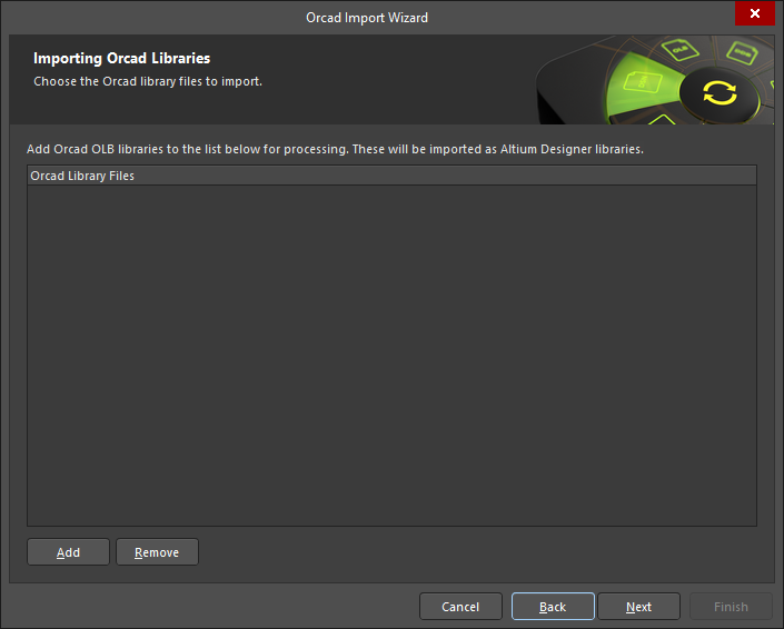
- Add any Schematic or PCB Libraries to import (if available).
- Set the options for what level of reporting is done after the translation has completed.

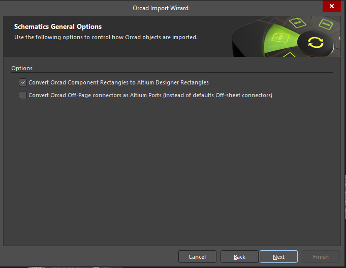
- Select whether you want to convert OrCAD component rectangles to Altium Designer Develop rectangles and use Off-Page connectors of OrCAD as Altium Ports.
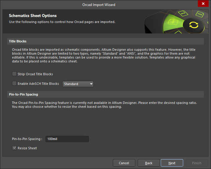
- Set your desired Schematic Sheet options, including how Title Blocks are imported and Pin-to-Pin spacing options.
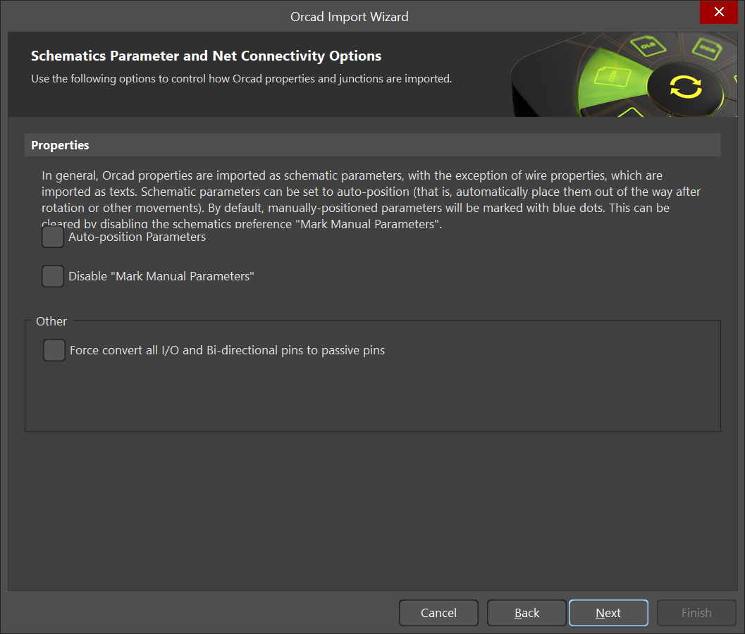
- Set your Schematics Parameter and Net Connectivity Options. Here you can choose to Auto-position the Parameters, and also Disable “Mark Manual Parameters”.
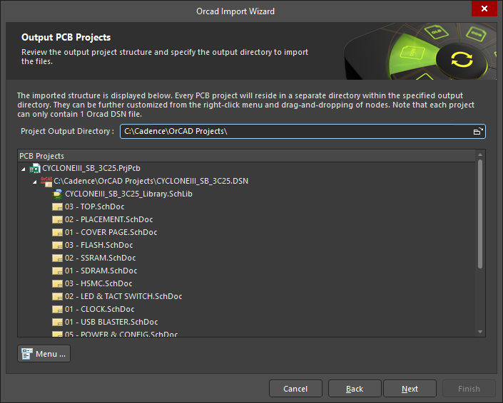
- You will see a preview of the files being translated and their output directories. You can change the main output directory if desired.
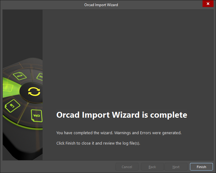
- Click the final Next button. The Import Wizard will take care of the rest.
- Congratulations, your design has now been imported into Altium Designer Develop!
- Follow the Post Import Tidy Up checklist to ensure the design has been fully reviewed and verified.
Phase 4: Post Import Tidy Up
Once your migration is complete, we recommend checking your design to ensure that all data is transferred as expected. Below is a list of key checks to perform post-migration:
Physical check
- View » Fit Document
- Board shape and cutouts
Electrical check
- Netlist
Rules
- Have all rules been imported
- DRC check
- Check settings for polygons - Island removal, min primitive size
- Thermal reliefs, direct connect
- Check power plane settings
- Power plane Pull-back
- Solder mask, Paste mask rules
- Via Tenting
- Testpoint assignments
Power check
- Nets
- Planes
- Polygons
Documentation check
- Layers
- Text/Strings
- Legends
PCB reports
- Number of components/nets
- All nets routed
Making a Smooth Transition from Cadence Allegro/OrCAD PCB Editor to Altium Designer Develop
In this guide, we’ll focus on importing Allegro/OrCAD Layout PCB designs. Please refer to specific guides if you need to migrate other files.
Phase 1: Prepare Original Data
It is prudent to clean up your design before attempting to export. Below is a checklist of data cleanup best practices to help you as you prepare your data:
PCB considerations:
-
Large numbers of graphical objects like mechanical drawing or non-ECO-registered drawing primitives must be migrated on documentation layers.
-
Star point grounding check.
-
Remove deliberate DRC violations.
-
Remove objects extending beyond the environment.
-
Known PCB layer assignments need to map correctly with existing Altium Designer Develop PCB, especially with the power plane or signal layer.
-
Do the auto-named nets match with the schematic?
Library considerations:
- Does 3D information need to be imported? If yes, then the height attribute should be assigned in Allegro.
- Correct representation of custom Allegro, copper shapes, solder mask, and resist?
Phase 2: Save Data in a Suitable Format
Supported Version and File Format
The following table shows the versions of all Allegro design formats that can be migrated into Altium Designer Develop. This list is updated regularly, so please check with us before starting a new migration. Refer to this link for updated information.
| TYPE | SYSTEM | VERSION | FORMAT |
| Schematic | Allegro | up to 17.4 | ASCII (*.alg) |
The Altium Designer Develop Import Wizard handles both Allegro PCB Design files (*.brd) and Allegro ASCII Extract files (*.alg). If you have Allegro PCB Editor installed, you can directly translate Allegro PCB Design files (*.brd) into Altium Designer Develop PCB files (*.PcbDoc)
PCB files translate to Altium Designer Develop as follows:
| ALLEGRO FILE TYPE | ALTIUM DESIGNER DEVELOP FILE TYPE |
| Allegro Binary PCB Design files (*.brd) | Altium Designer Develop PCB files (*.PcbDoc) |
| Allegro ASCII Extract Files (*.alg) | Altium Designer Develop Schematic file (*.SchDoc) |
Using ASCII Conversion to Import Without Allegro Installed on the Same Workstation as Altium Designer Develop
An Altium Designer Develop workstation with no licensed Allegro installation can import Allegro ASCII Extract files (*.alg). The following procedure enables a Licensed Allegro user to convert Allegro binary *.brd files to Altium compatible *.alg files. However, you must run this conversion on an Allegro-licensed machine.
- Locate the following two files in the \System folder of your Altium Designer Develop installation (Summer 08 or later):
• Allegro2Altium.bat
• AllegroExportViews.txt - Copy the two files to the folder containing the *.brd file.
- Open a command prompt, navigate to the folder containing these files and type the following: Allegro2Altium your_ file.brd (your_file = file name)
- Surround your filename with double quotes if the filename contains spaces, i.e., Allegro2Altium «yourfile.brd»
- Your Allegro-licensed machine will create an ASCII file will create an ASCII file and place it in the folder with a *.alg extension. Copy the *.alg file to the Altium Designer Develop workstation and import using the Import Wizard.
Phase 3: Import Data into Altium Designer Develop
Using the Import Wizard for Allegro Design Files
You can launch the Import Wizard from the Altium Designer Develop File menu. Follow the step-by-step instructions on how to use the Import Wizard throughout your data migration.
Step-by-Step Import Instructions on Importing an Allegro ASCII PCB Design file.
- Start the Import Wizard with File » Import Wizard
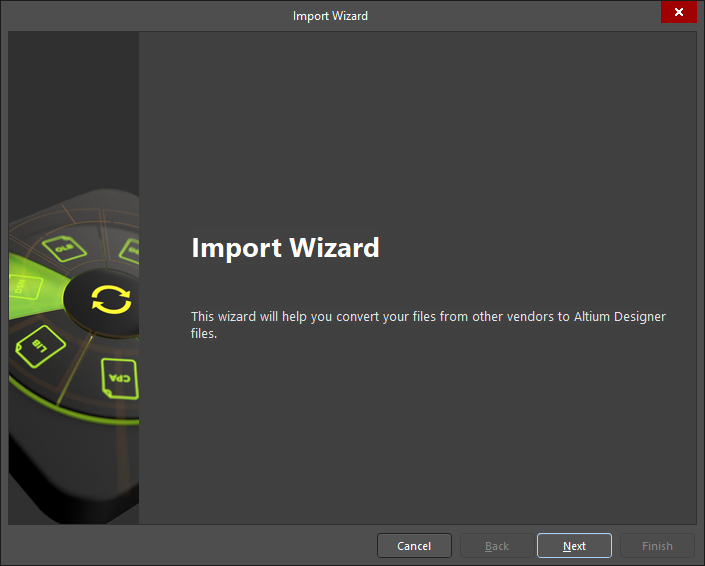
Starting the Import Wizard for Allegro files
NOTE:
You can also start the Import Wizard by dragging your Allegro Design Files into Altium Designer
Develop’s Projects Panel. This action will automatically launch the wizard in Allegro Import mode.
- Select Type of Files to Import—>Allegro Design Files
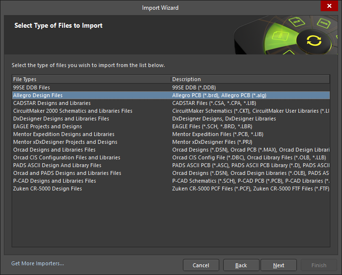
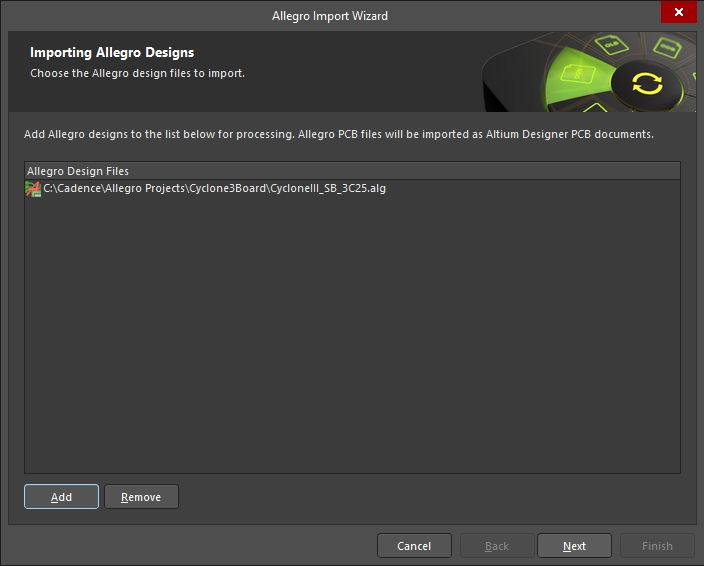
- Add the file(s) to be translated. In this case, ‘CyclonelII_SB_3C25.ALG’ has been used.
NOTE:
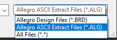
You can add as many *.brd and *.alg files as you like at this point. In the file browser, change the file
types pull-down to choose .brd or .alg files, depending on what you want to import. However, the
Import Wizard will create separate projects if you add different file types.
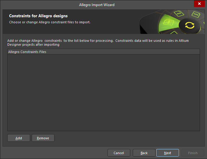
- Add Constraint File or Footprint —> If available and if you would like to add.
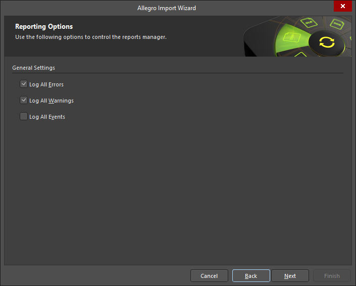
- Use the Reporting Options page to enable or disable the settings for logging all errors, warnings, and events, respectively.
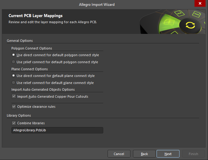
- The Import Wizard presents users with several options to control the translation from Allegro to Altium Designer Develop. Specify Polygon Connect and Plane Connect options for the PCB import process appear at this stage. Enable the Import Auto-Generated Copper Pour Cutouts option to import the auto-generated voids in Allegro PCB Editor as cutouts when the file is translated. The default options are displayed below.
Layer Mapping
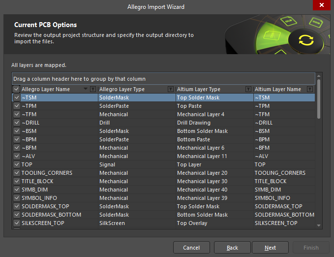
The Import Wizard provides the default mapping to build the layer mapping for each PCB. You can customize layer mapping for each design you choose to import. You may wish to import multiple Allegro PCB designs and map the same Allegro layer to the same Altium Designer Develop layer. You can set your layer mapping once and use this configuration for all of your import files if you want.
Setting layer mapping is an advantage because batch layer management can save time when importing multiple designs. The disadvantage to using layer mapping is that Default Layer Mapping is not always intelligent with differing structures in designs and may require some manual changes.
Right-click on the Altium Designer Develop Layer Mapping list (or use the dropdown) to manipulate the layer mapping of Allegro PCBs to Altium Designer Develop PCBs. You can even disable the layers which are not required on the Altium Designer Develop side or are not relevant. By default, the Import Wizard will map all layers.
You can use the Load and Save Layer Mapping Configuration Files command using the Load Layer Mapping and Save Layer Mapping menu items, respectively, to quickly apply layer mapping for Allegro and Altium Designer Develop layers.
Altium Designer Develop supports the default 30-layer mode and the expanded 250-layer mode for Allegro PCB files. If the user customizes the default layer mappings, those settings can be saved to a configuration file so that you can quickly reuse those mappings for subsequent translations.
- You will now see a preview of the files selected for translation, along with their output directories. You can change the main output directory at this point if desired.
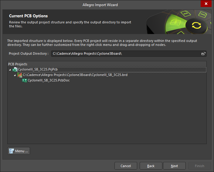
- Click the final Next button, and the Import Wizard will take care of the rest.
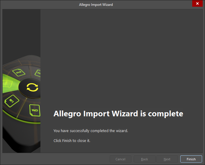
- Congratulations, your design has now been imported into Altium Designer Develop!
- Follow the Post Import Tidy Up checklist to ensure the design has been fully reviewed and verified.
- Make it to where you can view the link ‘Bringing Together Imported Schematic and PCB Designs’ guide.
Getting Help
There are many ways to learn more about Altium Designer Develop:
- F1 over any object, editor, panel, menu entry, or button to open a brief description in your web browser
- Press Shift+F1 or ~ key while running a command for a list of shortcuts you can use in that command.
- Access our complete Altium Designer Develop Documentation online.
- Visit the Altium Video Library where you can watch training on over 150 different topics. Each video walks you through the steps needed to complete a task.
- All Altium Designer Develop subscription levels include easy access to real-time support, user communities, comprehensive product documentation, training videos, and knowledge base of targeted solutions for common user experiences. Contact Altium Support Here.
Additional Resources
Online Resources:
If you’re ready to dive deeper into the powerful features of Altium Designer Develop, below is a list of articles that
provide information to help you get started.
- For a full overview of the PCB design process with Altium Designer Develop, check out this tutorial: A Complete Design Walkthrough with Altium Designer Develop.
- For a look at the basics of creating components, read A Look at Creating Library Components.
- For a tutorial that steps you through all the basics of editing multiple objects, take a look at Schematic Placement and Editing Techniques in Altium Designer Develop.
- For an overview of How to Start an FPGA PCB Layout in Altium Develop Designer, read How to Start an FPGA PCB Layout For Your Embedded System.
Software Platform Resources:
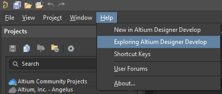
Another great way to get the most out of your Altium Designer Develop installation is by exploring its help section. You can launch the help menu on the left side of Altium Designer Develop by clicking Help and navigating to Exploring Altium Designer Develop.
Related Technical Documentation
Table of Contents
Design to Release, Without the Friction
- Keep reviews tied to the right version
- Reduce handoff confusion and rework
- Spot sourcing and release risk earlier
- Work solo, share when needed
Get Started
Thank you, you are now subscribed to updates.

