What Are the Advantages of Using Templates for PCB Design?

The domestication of horses, inventing the wheel and developing the combustion engine are tremendous milestones that we laud for enabling us to get around more efficiently and explore new places. Although, this is true another creation that deserves at least as much credit for giving most of us the confidence to branch out from our familiar surroundings is the map. The knowledge that someone before us has traversed a path gives us confidence in our own arrival.
PCB design is a creative process that can be filled with some trial and error. It is virtually impossible to eliminate these mistarts from the process; however, by using project templates we can minimize them. At the most basic, project example templates are effectively circuit “maps” that were designed previously that you can confidently use as a basis for your new design. In Altium Designer®, this basic concept has been expanded, but before looking at the many advantages of using project templates for PCB design let’s define this design reuse further and see how to create them.
What are Project Templates?
Project templates (sometimes called layout template or design template) are simply existing designs that have been previously created and are used to lessen the work necessary to design similar PCBs, PCB modules or individual components. Your board doesn’t always have to be that strenuous process of generation through PCB layout. When you have the circuit board already made, the job might be done easier. Templates may be used as is or they can be altered to accommodate specific requirements for your design, similar to reusing circuits for multi-channel design.
As in the case of multi-channel design, project example templates must be easily accessible to engineers, PCB designers, and other design team or organization members to be effective. Whether it is through schematic organization, footprints, or design templates - having a database of previously used board designs can speed up the process for your whole team.
Although, the software Altium Designer provides is flexible enough to store layout templates in any location project templates are typically located on a managed server, such as the Altium Vault®. Using a server not only provides a centralized storage location for the files but also has a well structured administrative control architecture in place. This is important for maintaining security and access level specificity.
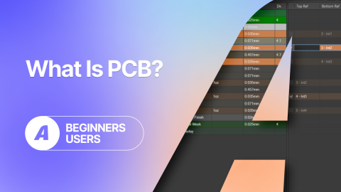
With any good PCB design software, you’ll have access to a directory of boards and project example templates to rely on. A sample directory structure for project templates housed in the Altium is shown below, in Fig. 1.
Fig. 1 Project template directory structure
As shown above, layout templates may be classified and stored as individual components, sheets (modules, schematics or PCBs) or complete designs (all components, schematic and PCB). It is for project templates to be stored with associated files that may include history, revisions, code and other documentation; therefore, all information and data can be viewed/downloaded from one location by accessing the template.
How do I Create Project Templates?
The difference between a single-use design and a reusable design that can serve as a project template lies in where and how the design files are stored. When designing a PCB it is typical to store all of the files under the project directory to provide easy access to all project files from a single location. In order to find a component or sheet, you would need to know within what project the design files exist. Obviously, this method of reusing designs quickly becomes untenable with evolving circuit board needs.
Thus, the need for simpler and more easily accessible means of locating designs that you wish to reuse. In Altium, layout templates are stored under a template directory structure where the actual files can be seen and accessed easily without the need to recall specific project directory names. Creating the project template and adding to the storage structure can be accomplished in three steps.
Steps to Create a Project Template:
Step 1: Create or select folder to store template
Whether you are creating a design template for a single component, a single sheet of a larger design or a complete design the first thing to do is to create its folder. This is done by right-clicking on the directory within which you want to create the folder. It is important that you define the folder type as this determines its classification and access. If necessary, you should also create or define the naming scheme and then set the folder properties, as shown in Fig. 2.
Fig. 2 Creating project template folder
Step 2: Create component, sheet or design template
Once you have the project template folder setup you next want to create the design itself and store the necessary files in the folder. Make sure content type for your design file(s) is set to Project Template. Now, your file(s) will be added to the Project Template listing when it is accessed for design reuse.
Step 3: Set Release Status
In order to allow others to access and modify your project template, the Revision State must be set to Released. This is indicated beside the green blocks in Fig. 3.
Fig. 3 Release status example
The Advantages of Using Project Templates
The ability to easily use and revise previous designs can significantly improve the productivity of you and your organization’s PCB design and development. Not having to completely create every design from scratch can translate into tremendous man-hour and cost savings. The advantages that your workflow can realize from using project templates and design reuse in Altium is determined by the degree to which embed the capability into your operations, but a few notable advantages are listed below.
Advantages of using Project Templates for PCB Design Reuse
Just as maps allow you to travel more efficiently, since you are not required to discover the best route project templates allow you to design efficiently and confidently and forego sourcing, laying nets and even coding. With Altium, you can fully utilize the advantages of using project layout templates for PCB design. Think of the possibilities with project templates on your board design and PCB layout like:
- Easily store and reuse components, modules, and complete designs.
- Detailed historical data and information
- Up to date tracking of project example template revisions.
- Quickly check accessibility status of the project template.
- View or download project template and associated files from a single location.
If you would like to test drive Altium 18, you can get a free trial here. If you want to learn more about the advantages of using project example templates in Altium 18, software engineering, or design reuse, talk with an Altium PCB design expert.
Related Resources


Related Technical Documentation

Table of Contents
Take advantage of the world's
most trusted PCB design system.
One interface. One data
model. Endless possibilities.
Effortlessly collaborate with
mechanical designers.
The world's most trusted
PCB design platform
Best in class interactive
routing
View License Options
Thank you, you are now subscribed to updates.