


What is a PCB and Intro to PCB Design


Printed circuit board (PCB) design has grown into its own specialized field within the electronics industry. PCBs play an important role in that they provide electrical interconnections between electronic components, rigid support to hold components, and a compact package that can be integrated into an end product. They are the main component in an electronic device that is responsible for form and function, and they allow advanced semiconductors to communicate with each other at very high data rates.
What is a Printed Circuit Board?
A printed circuit board (PCB) is an electronic assembly that uses copper conductors to create electrical connections between components. PCBs also provide mechanical support for electronic components so that a device can be mounted in an enclosure.
All PCBs are built from alternating layers of conductive copper with layers of electrically insulating material. Conductive features on printed circuit boards include copper traces, pads, and conductive planes. The mechanical structure is made up of the insulating material laminated between the layers of conductors. The overall structure is plated and covered with a non-conductive solder mask, and silk screen is printed on top of the solder mask to provide a legend for electronic components. After these fabrication steps are completed, the bare board is sent into printed circuit board assembly, where components are soldered to the board and the PCBA can be tested.
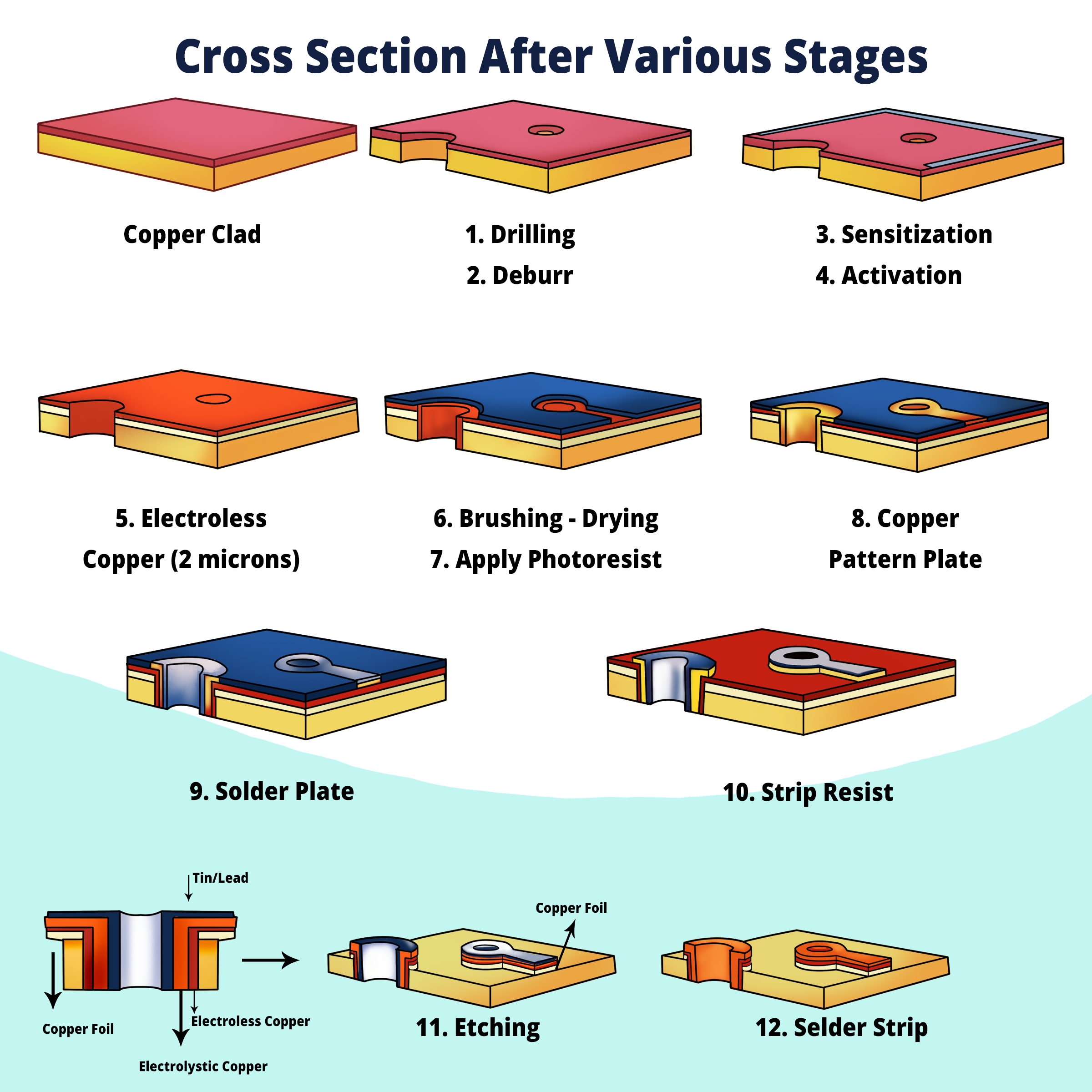
During manufacturing, the inner copper layers are etched, leaving the intended traces of copper for connecting components in the circuit board. Multiple etched layers are laminated in succession until the printed circuit board stack-up is complete. This is the overall process used in PCB design fabrication, where the bare board is formed before passing through a printed circuit board's assembly process.
PCBs Past and Present
Before we can explain PCB design, it is best to understand where PCBs have come from.
In the past, electronics were designed and assembled from small integrated circuits (ICs) and discrete components, which were connected together using wires, and the components were mounted to a rigid substrate. This original substrate was initially a material called bakelite, which was used to replace the top ply on a sheet of plywood. The number of wires was so great that they could get tangled or inhabit a large space within a design. Debugging was difficult and reliability suffered. Manufacturing was also slow, where multiple components and their wired connections were manually soldered.
Old PCBs often looked like the system shown below, where copper traces are exposed and many through-holes are used to hold large, bulky components.

Today, standard designs can have many small components, such as tiny ICs, very small passive components, and advanced chips with very high pin counts. It's impossible to manually connect all of these components together with soldered wires, so the copper connections are deposited directly on insulating substrates as described in the above manufacturing process. Many of today's devices are advanced high density interconnect (HDI) designs with thousands of connections and multiple electrical interfaces, powering everything from smartphones to heart rate monitors to rockets.
Types of PCBs
In the previous section, I focused on typical PCBs that are assembled on rigid substrates as these are the most common. However, there are other types of circuit boards that are constructed on a range of possible materials. The common types of these are:
- Single-sided - This board only has components mounted on one surface. The back surface is typically fully copper (ground) and coated with a solder mask.
- Double-sided - This type of circuit board has components mounted on both surfaces. Each surface is defined as a signal layer in the PCB stack-up, so the surfaces will contain traces that carry signals between components.
- Multi-layer PCBs - These boards have conductors on internal layers that carry electrical signals between components, or the internal layers could be conductive plane layers. Multi-layer PCBs may be single-sided or double-sided.
- Rigid-flex PCBs - Rigid-flex PCBs use a flexible polyimide ribbon that connects two or more rigid sections in a printed circuit board assembly. A rigid-flex board might be used when the design must have some movable element, such as a folding or bending enclosure.
- Flex PCBs - Fully flexible PCBs do not use any rigid materials and are made entirely of flexible polyimide ribbons. These boards can have components mounted and soldered on the, just like rigid and rigid-flex printed circuit boards.
- Printed flex PCBs - These PCBs use a flexible material as the base, and copper conductors are printed onto the flexible material in an inkjet process or in a similar additive process. The resulting boards are very similar to flex PCBs.
- Metal-core PCBs (or insulated metal substrate (IMS) PCBs) - These boards use a metal slab in the core layer (normally aluminum) in order to provide much greater rigidity and heat dissipation than in typical rigid printed circuit boards. The metal-core PCB design manufacturing process is quite different from the standard rigid PCB design manufacturing process, and there are a few design points to consider to ensure solvability. These boards are common in high-power lighting and some industrial applications.
- Ceramic PCBs - These boards are less common and are used in applications that require very high thermal conductivity such that the board can dissipate large amounts of heat away from components.
- HDI PCBs - These PCBs use very high pin count components that require a specialized manufacturing process and specialized materials to accommodate a very high density of copper connections.
- UHDI and Substrate-like PCBs - These PCBs are so small and dense that they have bypassed capabilities of subtractive etching, and instead they require a specialized additive manufacturing process used to build IC packages.
The fabrication and assembly processes for these types of PCBs vary, but today's ECAD software can help designers create any of these boards as long as the right PCB design rules are enforced in the software.

In the above image, we have an older circuit board that largely uses through-hole components to provide the required functionality. Modern printed circuit boards have switched to largely surface-mount (SMD) components as they are more useful in high-density, double-layer designs. SMD components are now the standard component type used in most applications that require a small form factor, low power, and low cost. However, some applications still make use of through-hole components as they are more reliable and easier to assemble, including with hand assembly. The image below shows an example of a modern PCB with high-density SMD components.

Structure and Applications of PCBs
Many of the important performance characteristics of a PCB are defined in the stack-up or the arrangement of layers in the PCB. The layer stack-up is built with alternating layers of conductive and insulating material, and with alternating layers of core and prepreg (two types of dielectrics used in the layer stack-up). The dielectric and mechanical properties of the core and prepreg will determine reliability and signal/power integrity in the design, and they should be selected carefully when designing for high-reliability applications. For example, military and medical applications need highly reliable designs that might be deployed in harsh environments, and a PCB for a telecom system might require a low-loss PTFE laminate in a small package.
An example of a PCB stack-up is shown below. In this example, the stack-up implements a 4-layer structure with two internal plane layers (L02_GND for ground, and L03_PWR for power). This type of stack-up is appropriate for IoT devices, lightweight embedded systems, and many other designs that use high-speed protocols. The internal plane arrangement helps ensure power integrity while also providing some shielding against external EMI. The internal plane layers also provide a consistent reference for controlled impedance signals. This type of stack-up is typical for many designs and is often a starting point for many modern printed circuit boards.

High-Density Interconnect (HDI) PCB Designs
Today's advanced devices in PCB design utilize high density interconnect (HDI) design practices, where the sizes of features in a PCB can be extremely small. These circuit boards largely follow the same engineering process as any other circuit board, but they are deployed in more advanced systems requiring large numbers of components and connections. Some of the well-known products where these circuits boards are used include:
- Smartphones and other mobile devices
- Data center architecture, such as server motherboards
- Add-in cards for servers and embedded computers
- Very small medical wearables or implants
The main component packaging type that can drive the use of HDI design and manufacturing in a PCB build is ball grid array (BGA) packaging, as well as related packaging types like land grid array (LGA). Many popular microcontrollers, MPUs, and FPGAs are offered in BGA packaging as this is the easiest way to fit a large number of I/O pins into a small component package size. BGA packages are the biggest drivers of miniaturization in many devices, and many consumer products use custom processors in BGA packages. For example, the image below shows the bottom side of an older CPU, but the supporting components on the IC substrate are visible from the bottom side.

Ultra-High Density Interconnect (UHDI) PCBs
The next generation of PCB design and fabrication marks a convergence with component packaging, which is used to hold semiconductor chips in ICs. Chips in advanced processors and digital/RF modules are placed on an IC substrate, which provides the interconnections between the electrical contacts on the semiconductor die and the PCB. The most advanced ICs are implementing feature sizes that are similar to features found in IC substrates, and the same manufacturing processes are used to produce both IC substrates and UHDI PCBs.
The small feature sizes used in UHDI PCBs are pushing the limits of many manufacturers, and currently these capabilities are only accessible at scale in Taiwan. However, global UHDI capacity is increasing due to significant investment by Western nations. The manfuacturer capabilities required to produce these boards are purely additive, where traces and vias are formed through metal deposition processes rather than through the subtractive etching methods used in conventional PCBs. These PCBs will also be the main drivers of the most advanced systems operating at the highest data rates. Although the production processes are very different, the process for designing UHDI PCBs is very similar to that for conventional PCBs.
Starting a New PCB Design
When it's time to start a new design, printed circuit boards pass through several stages. Production-grade circuit boards are designed using ECAD software, or a CAD application that includes many utilities that are specialized for circuit board design and layout. ECAD software is built to help designers walk through a specific process for circuit board design, beginning with basic electrical drawings and ending with manufacturing file preparation. Circuit board design follows a basic process:
- Front-end engineering - In this stage, the major components are selected and some basic circuit diagrams are typically created so that the functionality in the board can be designed.
- Schematic capture - This is the stage where ECAD software is used to translate simple circuit diagrams into electronic drawings that define electrical connections between components. Schematic symbols are used to denote components in the design.
- Material selection and PCB stack-up design - In this stage, laminate materials are selected and the stack-up is designed to accommodate the need for plane layers, signal layers, dedicated routing channels, and specific material properties.
- Component placement - After the board shape is set and components are imported into a new PCB layout, components are arranged in the layout to comply with the design's mechanical requirements.
- Routing - Once the component placement is approved, it's time to route traces between components. Routing tools in ECAD software are used to set Trace geometry may be determined in this stage with the goal of ensuring impedance control (for high-speed signals).
- Design review and verification - Once routing is completed, it's always a good idea to inspect and evaluate the design to ensure there are no mistakes or unresolved problems. This can be done with manual inspection or using post-layout simulation tools.
- Preparing for Manufacturing - Once the design is completed, it's time to prepare for production by generating standard manufacturing files. These files are used in automated fabrication and assembly equipment.
If you want to easily get through all of these stages in the PCB electronics board design process, you need to use the best design software with an intuitive user interface and a complete set of PCB design features.
Use Altium Develop to Create Your Printed Circuit Boards
The industry's best ECAD software should be easy to use and easy to learn, and it should include a complete set of design features. Altium Develop includes everything in a single platform, no external programs are needed to complete a design and prepare it for production.
- Altium Develop gives you everything needed to turn your ideas into reality. You can build anything from simple single-sided boards to advanced, high-density electronics.
- Altium Develop user interface is built on an integrated design rules engine that ensures your design features work together in a single program.
- Design teams use Altium Develop to stay productive and share design data in a secure cloud environment.

Altium Develop integrated design environment provides everything needed to design and manufacture high-quality printed circuit board assemblies. Other programs separate your important design tools into different programs with different workflows, making it difficult to stay productive and increasing your licensing costs. Altium Develop is consistently rated as the easiest to learn and the easiest to use, making it ideal for new designers and experienced professionals.
Whether you need to build reliable power electronics or advanced digital systems, use Altium’s complete set of PCB design features and world-class CAD tools. Altium Develop provides the world’s premier electronic product development platform, complete with the industry’s best PCB design tools and cross-disciplinary collaboration features for advanced design teams. Experience Altium Develop today!

About Author
Related Resources
Table of Contents
Design to Release, Without the Friction
- Keep reviews tied to the right version
- Reduce handoff confusion and rework
- Spot sourcing and release risk earlier
- Work solo, share when needed
Get Started
Thank you, you are now subscribed to updates.

