DC-Aware Return Current in Mixed Signal PCBs

One common high speed PCB design rule is: keep track of the return current path for your signals. This is actually a lot easier than it sounds, as the return path for a fast digital signal or even a moderate frequency analog signal is confined below the trace to a significant extent. At very low frequencies or DC, the return path could technically exist anywhere, which leads to some alternative routing practices you may see in audio designs, low frequency sensor interface designs, and pure DC systems. The ground plane only provides a benefit in terms of EMI shielding, but it doesn't confine the return path directly below traces.
There are some devices that operate at low frequencies or DC, and those devices also complete a circuit and therefore have a return path. So if you need to use one of these devices, and we suppose that the SNR value for the device is low, how can you ensure the return path loop does not create susceptibility to noise?
Here I want to show some ways you can work with these types of components, where a very low frequency signal or a DC signal needs to be measured, but the return path needs to be tracked to ensure the current loop is tight. We’ll examine some specific cases below.
Where is the DC Return Path?
Myself and many others have shown drawings such as that Illustrated below, which intends to show the difference between an AC return path along a trace and a DC return path for the same trace. Without going deeper into the physics, I’ll just state that it is well known that the AC return path is the path of least impedance, while the DC return path is the path of least resistance.
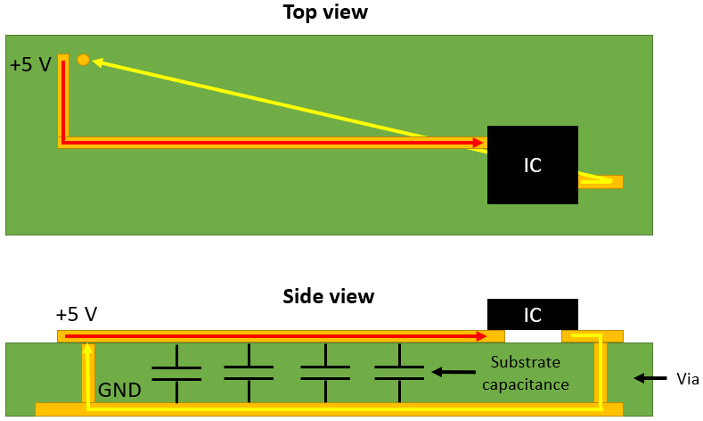
I created this return path drawing back in 2019 to conceptually illustrate what happens to DC currents flowing in a plane; learn more in this article.
With that small bit of information out of the way, now let's think about how to maintain DC return currents where you want them in specific situations. It should be clear that the DC return path could be anywhere including below the input trace (assuming a single-ended interface). This fact, as well as the conductor interface to your components, determines how the DC return path can be confined and you can achieve low noise at low frequencies. To see how this works with various analog components or sensors, let's look at some examples.
Sensor With a Differential Interface
Differential interfaces aren't just built for differential pairs carrying high-speed signals. Low frequency or analog interfaces can also be differential. The readout of the low frequency or DC signal in this case works the same way: the signal’s voltage is taken as the potential difference between the two conductors. Examples of these components include:
- RTD sensor
- Pressure sensors
- Output from a differential amplifier
- Position sensors
A similar idea applies in synthesis, where a design uses a DAC or a tunable DC source to generate a voltage which is then passed through an amplifier/driver with differential output. In either case, the factors determining noise received on this DC interconnect are the same.
This is arguably the easiest of the three cases shown in this article. The reason for this is quite simple: it is because you are routing a differential pair, and in this case the pair should be routed over ground. In DC, this differential pair totally confines the return current to the negative polarity portion of the interface. There is no switching, therefore there is no displacement current in a nearby ground plane, so we do not need to worry about tracking that portion of the return current. The standard differential pair routing rules apply here with the exception of length tuning.
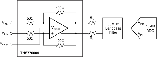
Differential amplifier and differential ADC interface. With a DC signal, each trace provides a complementary return path for the other trace. This image shows the THS770006 from Texas Instruments, but other differential components could be used in a DC sensor interface.
Two-Wire Sensor Interface With Common Ground
One recent example I worked with on a precision motion control project involved a pair of wires carrying out-of-phase sinusoidal waveforms. The analog front-end measures the difference between these two wires and a reference oscillator signal is used to extract the phase difference in order to very precisely determine the position of a small motor.
In this case, you do not have a true differential interface because you have two separate wires with a common ground. The common ground carries the return current while each of the wires carries part of a signal. When the SNR value is low, the ground region with the return current should be isolated from all other ground regions. One way to do this is to have small ground discontinuities around the sensor interface.
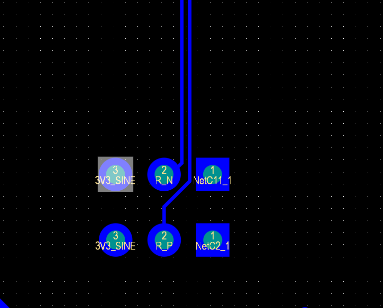
This 2-wire interface offers a simple way to provide noise control without requiring a true differential pair.
The other option in some cases is where you have groups of differential DC wires coming into the analog front-end. In the image below, I am showing inputs from a motor resolver from a D-sub connector. The left and right differential pairs are detected individually, and then the difference between them is used to determine motor position. Because the return path exists in corresponding wires, the ground cutout is not needed.
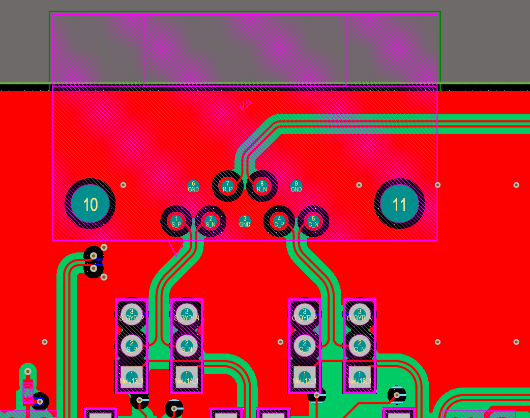
By cutting out some of the copper pour in your ground layer, you're controlling where DC return currents can exist. The constraint here is that you cannot route in the split area on any other layer. This would create problems with radiated emissions if any traces carrying signals are routed over the cutout region. A simple way to accomplish this is to define a keepout that overlaps on all layers so that no copper can be placed in the region around your two wire interface.
Interfaces With Common Power and Ground
In this type of interface, power and ground are shared across your PCB and the external device. There are two cases here:
- The external device sources power and signal to your PCB
- Your PCB sources power to your external device, and the device sources signal to your PCB
The first case is much easier to deal with as the power return point is directly to the external device. The management in this case is easiest when signal and power are shared on your connector as this forces the DC return path to be co-located with the DC/low-frequency signal. The return current for the low-level signal is confined to the cable/connector, which keeps it away from any other signals that might induce crosstalk.
The second case is more common and more complicated; the complete circuit loop will span up to the power regulator for your DC interface. So, the return path could be very unpredictable, and this might demand placing the supply much closer to the sensor interface. If you can do this, it is possible to create a region in the design where only the desired DC/low-frequency signals exist and the region can be kept resilient against noise.
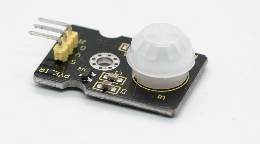
These small ultrasonic sensor boards take power from your host PCB and deliver signal over the same interface. This might create an opportunity for your signal to receive noise.
Whether you need to build reliable power electronics or advanced digital systems, use the complete set of PCB design features and world-class CAD tools in Altium Designer®. To implement collaboration in today’s cross-disciplinary environment, innovative companies are using the Altium 365™ platform to easily share design data and put projects into manufacturing.
We have only scratched the surface of what’s possible with Altium Designer on Altium 365. Start your free trial of Altium Designer + Altium 365 today.

About Author
Related Resources


Related Technical Documentation


Table of Contents
Take advantage of the world's
most trusted PCB design system.
One interface. One data
model. Endless possibilities.
Effortlessly collaborate with
mechanical designers.
The world's most trusted
PCB design platform
Best in class interactive
routing
View License Options
Thank you, you are now subscribed to updates.