


Everything You Need to Know About PCB Components

At a Glance
Learn everything you want to know about the components that go into a PCB. Your PCB design software helps ensure components can be assembled with minimal defects and rework.


PCB components are not just electronic parts, they are important pieces of data in ECAD software used to create a PCB layout. The physical components placed on a PCB during assembly all have digital analogs that exist in your PCB design software. As such, designers have a responsibility to know about the physical characteristics of their components and to create this data in PCB design software while ensuring DFM and DFA rules are followed in the component data.
This guide outlines PCB components from both perspectives: the physical parts that are placed in a PCB assembly and the digital representations that live in PCB design software. PCB components in Altium are some of the easiest to create thanks to an intuitive user interface and a footprint wizard that provides IPC-compliant footprints. Before you accept third-party footprints from unknown sources, read this guide to see what you should expect in PCB components in your design software.
Physical Electronic Components
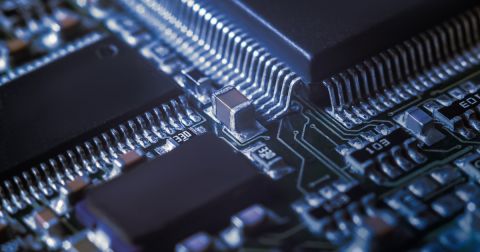
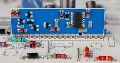
The power of today's PCB design software is that it supports designing with any electronic components or mechanical components. While the PCB component design features in PCB libraries prioritize electrical components, mechanical components can be supported as well and can be modeled using 2D boundaries and 3D models. Once placed in schematics and the PCB layout, these parts are automatically exported into the BOM for the product.
PCB components in your PCB design software are always digital representations of a physical component. Normally, we look at these in a 2D perspective so we can see the pad arrangement, silkscreen, solder mask openings, and paste mask openings. We can see other layers in a typical PCB footprint as well, such as in the example shown below.

The pad arrangement in a PCB layout is very important because it is required for soldering a component onto the PCB. In PCB assembly, we use soldering processes that can be scaled up to high volume with high throughput, and the pad arrangements used in PCB components are designed to ensure strong adhesion to the PCB as well as low defect rates in PCB assembly. The tasks involved span from mask opening design to sizing pads and ensuring sufficient clearances between PCB footprints and component bodies.
PCB design software helps you check these aspects of your PCB layout using a built-in design rule system. For example, the design rule system in Altium works in 2D and 3D, allowing DFM constraints to be checked and mechanical placement to be verified in a single system.

Physical components come in a variety of packages and form factors, and not all of these are standardized (in JEDEC for example) nor do they have a corresponding IPC standard guiding footprint design.
Common Surface-Mount Packages:
- SOIC (Small Outline Integrated Circuit) - Surface-mount equivalent of DIP packages with smaller pin pitch
- SOP (Small Outline Package) - Surface-mount packages smaller than SOIC, includes several variants:
- SSOP (Shrink Small Outline Package) - Smaller pin pitch than SOIC package
- TSOP (Thin Small Outline Package) - Thinner bodies than SSOP with pin spacings as small as 0.5mm, commonly used for memory modules
- TSSOP (Thin-Shrink Small Outline Package) - Same as TSOP but with lower height profile
- QFP (Quad Flat Package) - Surface-mount packages with pins extending from all four sides, supporting hundreds of pins:
- LQFP (Low Profile Quad Flat Package) - Lower height compared to standard QFP
- TQFP (Thin Quad Flat Package) - Even lower height than LQFP
- QFN (Quad Flat No-Leads Package) - Leads are located beneath the package with an exposed die-attached thermal pad, includes variants:
- TQFN (Thin Quad Flat No-Leads Package) - Thin version of QFN
- VQFN (Very Thin Quad Flat No-Leads Package) - Very thin version of QFN
- DFN (Dual Flat No-Leads Package) - Dual rows of pins instead of four rows
- BGA (Ball Grid Array) - Pins placed in grid pattern on under-surface using solder balls for connection, providing high density connections and superior thermal performance
- LGA (Land Grid Array) - Similar to BGA but uses flat contacts instead of solder balls for connection to PCB
- PGA (Pin Grid Array) - An older package common on CPUs, uses pins for connection to the PCB in a grid array pattern
- PLCC (Plastic Leaded Chip Carrier) - Features J-shaped terminals that can be soldered directly to PCB or used with PLCC sockets
Discrete Semiconductor Packages (SMD or Through-Hole):
- SOT (Small Outline Transistor) - Footprint for discrete surface mount transistors, diodes, and voltage regulators:
- SOT23 - Popular variation for lower power devices
- SOT223 - Used for higher power requirements with an exposed thermal pad
- SOD (Small Outline Diode) - Two-terminal package mainly used for diodes
- TO (Transistor Outline) - Through-hole packages for discrete semiconductors:
- TO-92 - Popular for transistors in hobbyist applications, low power handling
- TO-220 - Can dissipate more power and mount to heat sinks, used for voltage regulators
- TO-263 (D2PAK) - SMD equivalent of TO-220, can handle higher power dissipation
Schematic Symbols in PCB Components
All PCB components are represented in circuit drawings using schematic symbols, which detail the pins and electrical connections used to define circuits for an electronic device. Schematic symbols contain critical pieces of information:
- Pin names and numbers
- Component reference designator
- Sub-part number (for high pin count parts)
- Component description
- Metadata with electrical specifications
- Supply chain information
Some of the metadata (part number, supplier information, etc.) will be reflected into the PCB BOM once the manufacturing outputs are created from the finished PCB layout. Other properties in the schematic symbol metadata can be quite useful as they detail technical information about the component, such as power or temperature ratings, which can also be imported into the BOM.

Schematic symbols are also useful for building simulations in EDA software as a simulation model can be attached to a schematic symbol. While not all EDA software supports simulation inside a schematic drawing, the ability to perform SPICE simulations inside schematics is a major time saver as it eliminates a lot of duplicate work in a dedicated SPICE simulation program, such as Ngspice or LTSpice.
To build a schematic symbol for a PCB component, the designer simply needs to place pins, pin designators, and pin names on a component outline. Metadata is also added to the component as needed, but the supply chain information is required to prevent errors during procurement. The next step in PCB component creation is designing the PCB footprint.
PCB Footprints in a Layout
The schematic symbol only has a correspondence to the physical component in the PCB through the pin numbers, which are also reflected in the PCB footprint. The PCB footprint shows the 2D model of the pad arrangement that is required to make the physical copper connections to other components in the PCB layout. This is one of the primary reasons we create PCB footprints for use in a PCB layout.

The other major requirement for PCB footprints is that the pad arrangement balances component density requirements against the need for low assembly defect rates. A PCB footprint design is not guaranteed to eliminate defects, but the footprint does help prevent assembly errors which would normally require rework.
Just like a standard PCB layout includes multiple layers, PCB footprints also include layers, specifically conductor layers containing pads and copper features, as well as mechanical layers. The layers in PCB footprints have the same functions as in a PCB layout, and the information from the PCB component are automatically populated into the PCB layout. Layer functions are detailed in the table below.
| Layer Name | Description |
|---|---|
| Top Overlay/Silkscreen | Used for human-readable information like reference designators, component outlines, and part orientation on the top of the PCB. |
| Bottom Overlay/Silkscreen | Same as the top overlay, but for the bottom side of the PCB. Used less frequently unless components are mounted on both sides. |
| Surface Layers (Copper) | Defines the copper pads and traces for component connections on the top and bottom layers. |
| Internal Layers (Copper) | Defines copper features on the interior of the PCB. Used for routing in multilayer PCBs. |
| Top Solder Mask | A protective layer that covers copper on the top layer, exposing only the pads where components are soldered. |
| Bottom Solder Mask | Same as the top solder mask but for the bottom layer. |
| Top Paste Mask | Used to define openings in the stencil for solder paste application on SMT pads on the top layer. |
| Bottom Paste Mask | Same as the top paste mask but for the bottom side. |
| Mechanical Layer(s) | Used for outlines, dimensions, assembly notes, and manufacturing info. Multiple mechanical layers may be defined. |
| Courtyard Layer | Defines the physical space required by a component, including body, leads, and clearance for placement or automated assembly. |
| Keep-Out Layer | Specifies areas where copper routing or other components are not allowed. Used to enforce spacing rules. |
| Assembly Layer(s) | Contains component outlines and placement information used during assembly processes. Often used for pick-and-place and inspection. |
Typically, PCB copper and mask layers are defined using a footprint drawing in the component datasheet. Finally, once the PCB footprint is ready, a 3D model can be attached to the footprint data for use in MCAD applications.
Altium’s Tools For Creating PCB Components
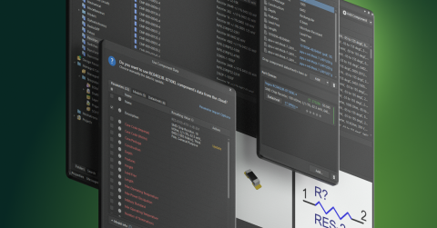
PCB component creation is a foundational part of product design, but there’s no reason the process should be difficult. To help designers speed through this process, Altium’s PCB design tools include the easiest component creation features, which allow fast creation of symbols and footprints in the cloud or in file-based libraries.
Altium’s components features give designers and librarians full control of footprints and the ability to comply with IPC standards on SMD parts and through-hole parts. Designers can also import realistic 3D component models from parts vendors, or quickly generate simple extruded models when vendor STEP files are unavailable.

To learn more about PCB component creation, view these resources:
You can also view our video on Altium Academy, featuring PCB designer and educator Phil Salmony. Phil shows how to use the IPC Compliant Footprint Wizard to quickly create IPC-compliant footprints for a new component. This simple tool greatly speeds up the design process for PCB designers and librarians, giving teams more time to focus building great products.
To ensure all team members can access component data, Altium’s cloud data management tools allow your components to be stored, shared, and tracked in version control. Every project can then rely on a single source of accurate and up-to-date PCB components, complete with technical data and supply chain information. PCB components have never easier to create, access, and mange in the cloud thanks to Altium.
Whether you need to build reliable power electronics or advanced digital systems, use the complete set of PCB design features and world-class CAD tools offered by Altium. Only Altium provides the world’s premier electronic product development platform, complete with the industry’s best PCB design tools and cross-disciplinary collaboration features for advanced design teams. Contact an expert at Altium today!

About Author
Related Resources
Related Technical Documentation
Table of Contents
Design to Release, Without the Friction
- Keep reviews tied to the right version
- Reduce handoff confusion and rework
- Spot sourcing and release risk earlier
- Work solo, share when needed
Get Started
Thank you, you are now subscribed to updates.